guido said:use one of the schematics without a GAL
Very funny ! 😀 😀 😀 😀 😀 😀
Non of that schematics is proofed to work and some are proofed to not work.

i will wait with this L+/L- R+/R- until someone of you provides something that will work.... and as i can´t make PCBs and will use protoboard 7 chips is little to much pins.
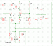
I build the following "D1 stage / 2 " and did tests.
Points marked "a" (sources) are trimmed with VR1 and VR2 to 0V.
With that stereopot i feed some current into the source, and measure voltage at points marke "b" and "c" (drains)
I get: With stereopot tuned for ca. 0mA :
b=13.5V c=13,6V
stereopot left: (+-3,25mA)
b=16,48V c=9,65V
stereopot right (-+3,25mA)
b=9,58V c=16,51V
given FETs are not matched and the stereopot may be far from beeing a precision device, i don´t see why this should work only with 0 to some mA. Why not also +- some mA?
Attachments
Feeding this stage does not wotk by simply connecting the TDA1543. I cut the Ri/v resistors, but i think the DAC wants to drice a higher resitance than it sees with this stage?
Question:
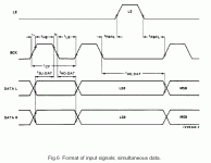
In the timing diagram the clock is interupted while the latch enable is high.
Is this a must ? Or did they draw it like this because at this moment the clock state is of no importance ?
Anyway, I guess I got it, will post in the morning, left channel with simple data line inversion for L-, mostly the same for right channel.
Attachments
rah said:Wow, this thread has grown huge!
I don’t know what happened to my subscription, I wasn’t even aware of all the things going on in here. 🙂
Anyway guys, like I promised before, that circuit I was previously working on is here. You know all about it from Ray’s (rfbrw) and my conversation on: http://www.diyaudio.com/forums/showthread.php?s=&threadid=25608
Today, after having a quick wiz through this thread, I thought I might take out some time and at least put something up. So here it is, I was working on it before, and have put in a document today. It’s a rushed job, bound to have mistakes! 🙂 But, hopefully you’ll find it useful. It has been simulated, graphs attached, but I have not tested it.
Keep up the good work on diyAudio!
Rahul.
It simulates correctly with 32Fs and 64Fs sclk and I see no reason why it wouldn't work with 48Fs though I haven't configured the dev board yet.
I was curious as to why you had two LE signals . As the dacs are running in stopped clock mode which effectively puts both datastreams in the same timeframe they should have a common LE signal. Having two may well confuse the unwary.
On the the subject of btc inversion. Digital audio dacs definitely have a bipolar zero and the +1 addition applies. i.e +1 = 00//01 and -1 would be 11//10 +1 = 11//11. What they also have are unequal Full scale values with the positive FSV being 1LSB step less than the negative FSV. A 4-bit code would range from +7 to -8.
ray

Hi Ray,
That would be an artifact of my symmetrical thinking! 🙂
Yes, it would be ideal to have just one LE that is signaled after both left and right DACs have been loaded. Just quickly looking at it now, I don’t see a simple way without adding more gates, but if you see a clever way, let us know.
I didn’t give this too much thought, but yes DACs do have a bipolar zero.
What I was thinking, was purely in terms of number systems. In 2’s complement if you invert the largest negative integer, it’ll overflow. Eg. in a 4-bit system, -8 is 1000, inverted 0111, add 1 and it becomes 1000 (+8), but in 4-bit 2’s complement it has overflowed and wrapped back to –8, clipping.
I was curious as to why you had two LE signals . As the dacs are running in stopped clock mode which effectively puts both datastreams in the same timeframe they should have a common LE signal. Having two may well confuse the unwary.
That would be an artifact of my symmetrical thinking! 🙂
Yes, it would be ideal to have just one LE that is signaled after both left and right DACs have been loaded. Just quickly looking at it now, I don’t see a simple way without adding more gates, but if you see a clever way, let us know.
On the the subject of btc inversion. Digital audio dacs definitely have a bipolar zero and the +1 addition applies. i.e +1 = 00//01 and -1 would be 11//10 +1 = 11//11. What they also have are unequal Full scale values with the positive FSV being 1LSB step less than the negative FSV. A 4-bit code would range from +7 to -8.
I didn’t give this too much thought, but yes DACs do have a bipolar zero.
What I was thinking, was purely in terms of number systems. In 2’s complement if you invert the largest negative integer, it’ll overflow. Eg. in a 4-bit system, -8 is 1000, inverted 0111, add 1 and it becomes 1000 (+8), but in 4-bit 2’s complement it has overflowed and wrapped back to –8, clipping.
rfbrw said:Err,Guido, it does not work. For a start the 4-input and-gate is clocked with WS and WS inverted which in practice means its output is always low. There is also WS delayed by a flip-flop clocked with inverted serial clock which causes a runt pulse in the data. But that can all be remedied.
What cannot be so easily dealt with from the CDPro2 point of view is that the circuit assumes serial clock is 64Fs. The CD Pro2 outputs a serial clock of 48Fs.
ray.
Thanks for your feedback. Had a look at the GAL content and the use of WS and WSdelayed. And i got as confused as you were....
What happend, i think, is that i started off without differential. For this case i did not need the WSdelay signal. Only:
DATA-R: WS * data + /WS * SHIFT32. This is possible because WS starts before the dataframe (1 clockpulse) and lasts for a number of clockpulses after the dataframe (WS=32 clockpulses, data is only 16). So there was no need for me to get WSdelay, WS was 'good enough'.
Much later i started to look at differential mode. Without it, nothing changed for the GAL listing. But with it i created WSdelayed to do the inversion in good way. Guess i could
have got away with WS actually. So one FF too many on the pcb,
a well their not that expensive. But now it is there, i'm going to use it.
Made some new timing diagrams and it looks like the line
/WS * WSdelay is only true at times that there is no valid dataframe: only the clockcycle before the MSB. So it is not used.
So in practice:
normal mode: data and shift32 are used.
differential mode: data and /shift32 are used.
(data and shift32 is the same data, just at another point in time).
So.... I guess the GAL content can be simplified:
DATAR :=
WSdelay * DATA * MUTE +
/WSdelay * SHIFT32 * DIFFERENTIAL * MUTE +
/WSdelay * /SHIFT32 * /DIFFERENTIAL * MUTE
Same for the R channel, but then with shift32 and shift64.
Looks much better i guess! Easy for me to test this out, if the above is ok. Only requires some GAL reprograming. Only a simplification inside the GAL. Nothing changes to the functionality.
So for the design without GAL we need to make (no normal mode, no mute):
DATAR := WSdelay * DATA + /WSdelay * /SHIFT32
WSdelay and /WSdelay come from the same FF, so we only need two AND's and one OR. In practice one NAND ic. So instead of 74F64 something that is not in the catalogues. I'll make a new schematic for this. And as i said somewhere above, using WS could already be enough. So no FF needed to make WSdelay and
just use another gate of the inverter.
We might end up with 2 working and easy schematics without GAL and one with GAL that is actually understandable.. 😀 😀 😀
Sorry for all the confusion
 Seems i am good at making things complicated

Feedback?

Rah,
LLE should be used for both channels and looking closely at the timing diagram FRAME16,both LE signals and both SCK signals start one SCK cycle too late.
ray.
LLE should be used for both channels and looking closely at the timing diagram FRAME16,both LE signals and both SCK signals start one SCK cycle too late.
ray.
We might end up with 2 working and easy schematics without GAL and one with GAL that is actually understandable..
that would be absolutely great!
guido said:
Sorry for all the confusion
Feedback?
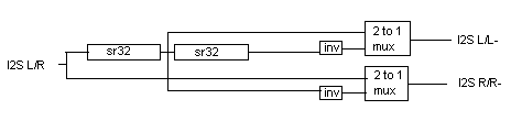
It certainly seems that way. So below is the outline of something a bit simpler.
Attachments
The CD Pro2 outputs a serial clock of 48Fs.
But the 2*32sr would cut a 48FS signal into fragments ?
Is ensured the right and left samples belonging to each other by the LE managment not shown in your outline? or does it produce an offset between samples.
till said:
But the 2*32sr would cut a 48FS signal into fragments ?
Is ensured the right and left samples belonging to each other by the LE managment not shown in your outline? or does it produce an offset between samples.
You could have taps at 24th flip-flop or use three 8bit shift registers instead of four... The input-select part of the mux is not shown and there is no offset between samples.
ray.
rfbrw said:
LLE should be used for both channels and looking closely at the timing diagram FRAME16,both LE signals and both SCK signals start one SCK cycle too late.
ray.
Ok, now I see what you meant before. The state of the LE signal doesn't matter because the clock will only clock in the correct data...
All those sigals (FRAME16, both LE signals, and both SCK) are
delayed by one SCK, and so is the DATA. All outputs get delayed
by one SCK...
Ray,
Just had a look at the image you posted in Post #211.
I had thought about doing the same before, and with
48Fs data I was going to use 3 x 8bit registers, but I
counted up the number of ICs, and it was no less 🙁
Of course it is much more simpler...
Just had a look at the image you posted in Post #211.
I had thought about doing the same before, and with
48Fs data I was going to use 3 x 8bit registers, but I
counted up the number of ICs, and it was no less 🙁
Of course it is much more simpler...
Rah,
If one assume WS in the last row corresponds to data in the second row then the MSB of the word is bit 5. That being the case, LCK does not start clocking data until bit6 missing the MSB by one.
If one assume WS in the last row corresponds to data in the second row then the MSB of the word is bit 5. That being the case, LCK does not start clocking data until bit6 missing the MSB by one.
review please:
Is it better to make 2 separate powersupplys for both sides of the CS8412?
Is the TDA1543 able feed the D1 stage, or does it need to see a higher resistance (1,1k)
Is it better to make 2 separate powersupplys for both sides of the CS8412?
Is the TDA1543 able feed the D1 stage, or does it need to see a higher resistance (1,1k)
An externally hosted image should be here but it was not working when we last tested it.
Is it better to make 2 separate powersupplys for both sides of the CS8412?
I don't comment if it's any better but if you do that make sure to put 2 diodes in antiparallel between those supplies to avoid latch-up at power-on ( as discussed in several previous threads ). Decouple the CS well. Check the Kusonoki DAC schematics to see what I mean with the diodes.
Before you ask it; use a good input transformer 😉
rfbrw said:Rah,
If one assume WS in the last row corresponds to data in the second row then the MSB of the word is bit 5. That being the case, LCK does not start clocking data until bit6 missing the MSB by one.
WS in the last row does correspond to the data in the second row, however the output data (datal_p, datal_n) is one BCK cycle behind data. This is why datal_p (the positive phase) "looks" to be out of phase with data, it's running behind.
rah said:
WS in the last row does correspond to the data in the second row, however the output data (datal_p, datal_n) is one BCK cycle behind data. This is why datal_p (the positive phase) "looks" to be out of phase with data, it's running behind.
Unless we are looking at two very different schematics, there is no delay applied to DATA.
- Status
- Not open for further replies.
- Home
- Source & Line
- Digital Source
- TDA1541A/S1 Arrangements