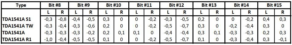
I checked the DNL error of various TDA1541A grades: S1, Taiwan, no mark, and R1. From bit #0 to bit #7 the error is <0.1 LSB for all grades. These bits are not included in the table.
The full scale THD shows some minor difference:
S1: 0.00026% / 0.00030% (L/R)
TW: 0.00039% / 0.00040%
no mark: 0.00037% / 0.00032%
R1: 0.00033% / 0.00037%
The full scale THD shows some minor difference:
S1: 0.00026% / 0.00030% (L/R)
TW: 0.00039% / 0.00040%
no mark: 0.00037% / 0.00032%
R1: 0.00033% / 0.00037%
Attachments

Hi thanks,
which year for the Taiwan, please ?
Now you have a S1 (if non taiwan) & a Taiwan no grade, are you not surprised they sound so different ? I was amazed by that !
which year for the Taiwan, please ?
Now you have a S1 (if non taiwan) & a Taiwan no grade, are you not surprised they sound so different ? I was amazed by that !
THD at -60 dBFS, S1 chip, before/after DNL optimization:
Bit 10: 0.29/0.19%
Bit 11: 0.22/0.19%
Bit 12: 0.34/0.24%
Bit 13: 0.32/0.22%
Bit 14: 0.25/0.17%
Bit 15: 0.40/0.20%
Bit 10: 0.29/0.19%
Bit 11: 0.22/0.19%
Bit 12: 0.34/0.24%
Bit 13: 0.32/0.22%
Bit 14: 0.25/0.17%
Bit 15: 0.40/0.20%
Seems worthy of implementing, so any chip can be deduced to ~same spec. There are any many non standard resistor values in smd, so trimpot can be used to figure out values, then replace. This way, it's less noise, and no worries that values will drift too much, at a much much lower cost than.
Honestly, costs almost nothing, and thd improvement's are great. Implementation is easy with using socket for trimpot, measure and replace with resistors. And use just that one trimpot to measure all, so quite cheap. Now, only caveat is that, one making this needs to have knowledge and gear to measure. This would especially work great in a temp controlled enviroment, like with mvaudio approach using temperature probe and noiseless noctua fan. So no deviations no matter the summer/winter.
I agree that the SMD resistor realization is more stable. But it is not possible to tune for minimum THD each bit (only bit 10 to bit 15) separately, because they interact.
The correct procedure is: tune bit 10 for lowest THD, then keep the variable resistor at this position, then move to bit 11 and do the same with the next variable resistor, then move to bit 12, etc. until bit 15.
The alternative method using +/-1 LSB step around each bit can be used independently for each bit 1 to 15 (whereas only bit 10 to bit 15 can be adjusted for exactly 1 LSB step).
After you have done, you can measure and replace all 2x6 variable resistors to SMD.
If tuning the upper 6 bits is too difficult, I recommend tuning only the MSB i.e. bit 15. This is the bit that flips at analog zero crossing, that has most influence on the THD at very low signal level.
Still not expensive if using bourns 10k multiturn, as it won't stay in that place as final resistor. And those are useful to have in a drawer always.
Imo it should be done on a pcb just made for that with the trim that stay in lieu. Then since you have the value put the chip in the final pcb with the according value with the hope there is a close value in the resistors catalog.
I have made the pcb à la Thorten, there is really no place left nowhere if you want small loops.
Will be interresting to see the correlation with the sound to check the quantity of improvment that can be hear beyond the numbers.
I have made the pcb à la Thorten, there is really no place left nowhere if you want small loops.
Will be interresting to see the correlation with the sound to check the quantity of improvment that can be hear beyond the numbers.
I measured the compensation voltage again. It seems the S1 grade needs only very little compensation.
Default voltage on the DEM capacitor / optimal compensation voltage before 10 M resistor
pin 23 (bit 10): -3.91 V / -3.78 V
pin 22 (bit 11): -3.95 V / -3.95 V
pin 21 (bit 12): -5.32 V / -5.58 V
pin 20 (bit 13): -5.56 V / -5.42 V
pin 19 (bit 14): -7.72 V / -7.72 V
pin 18 (bit 15): -7.58 V / -7.28 V
There is no difference in full scale THD, but the -60dB THD dropped to half. Next I will measure the "worst" i.e. R1 grade.
Looking forward to see the number of a normal grade Taiwan with an european S1. IMHO you should give the production year of the ship tested that ! 🙂
Soundwise, many noticed a bigger change when the heatsink was grounded to dgnd arguing about a better shielding.
But I strongly wonder if instead it is not due to the local Gnd reference reenforcment here.
I wanted to try with both the heatsink on the TDA and aside to experience that theory...
If yes the heatsink tailored to do a clean path with very low impedance between Dgnd and Agnd. Worth to try with just a thick wire first.
Same external trick could be used with wire between some pins, I think about the -15v pin local ground which if I followed well has a double dependancy with both Agnd and Dgnd pins ( external path through the gnd layer).
I remember you made a very usefull shematic on how the currents flows from the TDA pins.
Coul be interresting if it has dependency with DNL results ?
Last edited:
- Home
- Source & Line
- Digital Line Level
- TDA1541A reducing DNL