Bernhard said:
Because my simulator gives 1-1.8V
It is not possible to swing 200mV around 1.4V with 2 diodes.
2 diodes give 1.2V @ 1mA in my simulator
I get 1.35V with 1ma
Using simetrix's 1n4148's model
This gives me 1.2-1.6V:
Attachments
i think the indivudual preferred voodoo regulator everyone could drop in as he wants, what i want to know is, is the principle of I2S input preconditioning and the power suppys / filter / decoupling scheme rightUse LM431s instead of the zeners
till said:
i think the indivudual preferred voodoo regulator everyone could drop in as he wants, what i want to know is, is the principle of I2S input preconditioning and the power suppys / filter / decoupling scheme right
It should
just:
-I don't agree with the I2S input preconditioning resistors values
-I would use another +5V regulator for the I2S, one for the 3, not one for each one
Why all the hassle ?
Build it, adjust the resistors with a scope and that's it.
I will measure distortion with this mod.
Build it, adjust the resistors with a scope and that's it.
I will measure distortion with this mod.
till said:please give better values
Bernhard's right, we will have to build it and see the result.
If we have such differences with simulations, in the real world it would be even worse. I'm not sure we can give universal values.
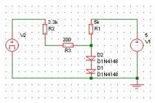
In simetrix, that's what I've found in order to get 1.2-1.6V (resistors name based on Bernhard's schematic)
R1=5k
R2=3.3k
R4=200
OR
R1=2.5k
R2=1k
R4=37
Pedja said:This leads mo to the conclusion a local decoupling between the pin 15 (-15V) and the pin 26 (-5V) could be welcome.
Also, putting aside the last possibility you mentioned, the pin 28 (+5V) should have nice AC path to the analog ground.
However, with existing decoupling of all the rails to ground and decoupling directly between +5V and -5V things are becoming a bit horrible.
Thanks,
Pedja
Looking at this and marantz cd7 schematic, it could be best to make -5 out of -15. Done at marantz CD7 with zener/transitors.
About all the decoupling. I'm thinking to only use:
-5 to -15 (current reference generator), -15 to dgnd (hf spike) and agnd to +5 (audio).
digital currents don't disturb the powersupply lines so much, so treat supplies as analog and use different +5 for other logic (and 1.3/1.5 V circuits). No direct caps between -5 to gnd or -5 to +5, "logic is nearly constant, except for spike" 😎😕
Now something funny, with a balanced dac L+R at +5 become
L+-L and R+-R, so ~0. 😀 😀 😀
That's where i am at, at the moment,
Gr
This might be done because of practical reasons as well. What could be the benefit of it instead of two independent regulators? Note that the scheme used by Marantz divides the current in two loops (input and output), it is the buffer. As any regulator does divides the loops, if it worth anything. 😉guido said:Looking at this and marantz cd7 schematic, it could be best to make -5 out of -15. Done at marantz CD7 with zener/transitors.
I assume in itself that the supply for the current reference generator should have the ends of its supply quiet in respect to each other, but also in respect to the ground, and it is the analog ground. Note also that the -15V is still most analog supply here and it has the weakest PSR.About all the decoupling. I'm thinking to only use:
-5 to -15 (current reference generator), -15 to dgnd (hf spike) and agnd to +5 (audio).
digital currents don't disturb the powersupply lines so much, so treat supplies as analog and use different +5 for other logic (and 1.3/1.5 V circuits). No direct caps between -5 to gnd or -5 to +5, "logic is nearly constant, except for spike" 😎😕
WRT the general idea you’ve exposed, if we assume that the digital inputs must be referred to the digital ground thus making sure the loop of the digital inputs won’t overlay with any other loop, and treat all the other supplies like the analog ones, we could easily finish with one huge classic ground fill beneath the chip. In this case, the supply regulators would be positioned right beside the pins they feed and would be referred to the mentioned ground fill. With decent regulators and caps of 100uF or 47uF (or less), not a lot of job will be left for eventually additional HF decoupling. It might be checked by putting small caps here or there if they are needed or not. Hmm, KISS TDA1541A layout...
I’d say yes, assuming these currents are occurring simultaneously.Now something funny, with a balanced dac L+R at +5 become
L+-L and R+-R, so ~0. 😀 😀 😀
I am at the idea to try to cross the bypasses in a few ways and to listen if something happens…That's where i am at, at the moment,
Gr
Pedja
Henk, Guido or someone please help ...
So far, I am still very much confused.
In order to provide individual power supply to the 3 power pins, and make separate returns, how do one pair up the pins? There are 3 supply pins (+5V, -5V and -15V), but only 2 returns (AGND and DGND).
So here is goes:
-15V pair with AGND (since -15V is pure analogue)
+5V pair with ???? (AGND or DGND?)
-5V pair with ???? (AGND or DGND?)
I understand that both AGND and DGND will be connected together at the end of the day, but I still like to know the proper pairing of the pins.
Please help 🙂
Re: Henk, Guido or someone please help ...
We all are trying to figure that out (at least i am). For now: -15 is analog, but -5 is analog (current generator between -15 and -5) and also digital (together with +5). Digital between +5 and -5, however analog currents also pop out of +5. And this is the short version... AGND and DGND should be connected at the DAC.
For now, i think it is better to decouple -5 to -15 and then -15 to GND (so the spike from i2s into -15 does not go through the loop of -15 and -5, where it would be if -15 and -5 are both decoupled to gnd). And then create -5 out of -15 to keep that loop small.
The caps at for dem decoupling goto agnd.
Confusing, i know
And then we did not even mention dem reclocking and creating small voltage i2s signals....
pop11 said:So far, I am still very much confused.
So here is goes:
-15V pair with AGND (since -15V is pure analogue)
+5V pair with ???? (AGND or DGND?)
-5V pair with ???? (AGND or DGND?)
I understand that both AGND and DGND will be connected together at the end of the day, but I still like to know the proper pairing of the pins.
Please help 🙂
We all are trying to figure that out (at least i am). For now: -15 is analog, but -5 is analog (current generator between -15 and -5) and also digital (together with +5). Digital between +5 and -5, however analog currents also pop out of +5. And this is the short version... AGND and DGND should be connected at the DAC.
For now, i think it is better to decouple -5 to -15 and then -15 to GND (so the spike from i2s into -15 does not go through the loop of -15 and -5, where it would be if -15 and -5 are both decoupled to gnd). And then create -5 out of -15 to keep that loop small.
The caps at for dem decoupling goto agnd.
Confusing, i know
And then we did not even mention dem reclocking and creating small voltage i2s signals....

Re: Henk, Guido or someone please help ...
The TDA1541(A) has the digital input circuits refered to a slicing level. This level is 2vj, thus two forward biased junctions above digital ground. All internal logic current routing logic and is refered to dgnd, and is supplied between -5V and +5V. Apart from some spikes, the logic supply currents are dc currents.
I expect that the PSR is much better if the voltage difference between -5V and -15V is kept constant while measuring the PSR of the negative supply. Keep in mind that the process is bipolar and that all npn collectors are junction isolated to the substrate, that is, to the -15V.
Yes, agreed.
The dac is can be seen as a digital controlled differential pair with a bias current of 2mA and a maximum current swing of 4mApp. One output is the dac output, the outher flowing into the +5V. The agnd is reference for the analog part including the diode/darlington switches of the binairy weigthed currents. There is no signal current in agnd, the dac current flows in, or into the output, or into the +5V.
It is possible to re-route the output current into the 5V node.
1. The well known voltage to current converter is made with an opamp, the +input of the opamp to agnd and a resistor between -input and opamp output. If the opamp has the +supply at the +5V of the dac, the dac's output current is re-routed in that +5V. The +5V sees only dc current.
2. In case of e.g. a small conversion resistor to agnd is used, the voltage can be sensed and converted to current again. This current, not the one to listen to, can routed into the +5V supply of the dac. The +5V sees only dc current.
These to examples form a very effective means to reduce the decoupling requirements or to improve the +5V decoupling.
In general, I agree to decouple all supplies to agnd. It is very important to know where currents flow. The return currents takes the shortest path, also in a ground plane. The return runs beneath the trace where the current flows. With a magnetic probe, this can be shown easely. As Padja stated, current padths should not cross.
regards,
pop11 said:So far, I am still very much confused.
In order to provide individual power supply to the 3 power pins, and make separate returns, how do one pair up the pins? There are 3 supply pins (+5V, -5V and -15V), but only 2 returns (AGND and DGND).
......
I understand that both AGND and DGND will be connected together at the end of the day, but I still like to know the proper pairing of the pins.
Please help 🙂
The TDA1541(A) has the digital input circuits refered to a slicing level. This level is 2vj, thus two forward biased junctions above digital ground. All internal logic current routing logic and is refered to dgnd, and is supplied between -5V and +5V. Apart from some spikes, the logic supply currents are dc currents.
Pedja said:I assume in itself that the supply for the current reference generator should have the ends of its supply quiet in respect to each other, but also in respect to the ground, and it is the analog ground. Note also that the -15V is still most analog supply here and it has the weakest PSR.
I expect that the PSR is much better if the voltage difference between -5V and -15V is kept constant while measuring the PSR of the negative supply. Keep in mind that the process is bipolar and that all npn collectors are junction isolated to the substrate, that is, to the -15V.
Pedja said:
WRT the general idea you’ve exposed, if we assume that the digital inputs must be referred to the digital ground thus making sure the loop of the digital inputs won’t overlay with any other loop, and treat all the other supplies like the analog ones, we could easily finish with one huge classic ground fill beneath the chip.
Yes, agreed.
The dac is can be seen as a digital controlled differential pair with a bias current of 2mA and a maximum current swing of 4mApp. One output is the dac output, the outher flowing into the +5V. The agnd is reference for the analog part including the diode/darlington switches of the binairy weigthed currents. There is no signal current in agnd, the dac current flows in, or into the output, or into the +5V.
It is possible to re-route the output current into the 5V node.
1. The well known voltage to current converter is made with an opamp, the +input of the opamp to agnd and a resistor between -input and opamp output. If the opamp has the +supply at the +5V of the dac, the dac's output current is re-routed in that +5V. The +5V sees only dc current.
2. In case of e.g. a small conversion resistor to agnd is used, the voltage can be sensed and converted to current again. This current, not the one to listen to, can routed into the +5V supply of the dac. The +5V sees only dc current.
These to examples form a very effective means to reduce the decoupling requirements or to improve the +5V decoupling.
In general, I agree to decouple all supplies to agnd. It is very important to know where currents flow. The return currents takes the shortest path, also in a ground plane. The return runs beneath the trace where the current flows. With a magnetic probe, this can be shown easely. As Padja stated, current padths should not cross.
regards,
We all are trying to figure that out (at least i am). For now: -15 is analog, but -5 is analog (current generator between -15 and -5) and also digital (together with +5). Digital between +5 and -5, however analog currents also pop out of +5. And this is the short version... AGND and DGND should be connected at the DAC.
I guess I am really really dumb, please bear with me
Can I say:
-15V pair with AGND (since -15V is pure analogue)
-5V pair with AGND (more Analogue than Digital?)
+5V pair with DGND (more Digital than Analogue?)
For now, i think it is better to decouple -5 to -15 and then -15 to GND (so the spike from i2s into -15 does not go through the loop of -15 and -5, where it would be if -15 and -5 are both decoupled to gnd). And then create -5 out of -15 to keep that loop small.
I don't get this, can you kindly explain it a bit more, please please
WRT the general idea you’ve exposed, if we assume that the digital inputs must be referred to the digital ground thus making sure the loop of the digital inputs won’t overlay with any other loop, and treat all the other supplies like the analog ones, we could easily finish with one huge classic ground fill beneath the chip.
Now I undrstand a little bit, although this goes a bit against what Kuei (Thorsten) has suggested.

So now where should the digital ground connected to the analogue ground?
It cannot be connected to the ground fill otherwise current loops will overlap, right?

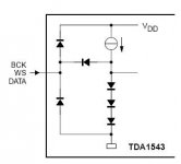
Bricolo said:Mr ten Pierick,
While reading the TDA1543's datasheet, I found this schematic representing how the inputs are made.
Unfortunately, there's no such schematic in the TDA1541A's datasheet.
It it similar (maybe with 2 diodes instead of 3)?
WS, BCK and DATA inputs of the TDA1541(A) are made by the base of a horizontal pnp. They have a one diode, the base to substrate junction, to -15V.
regards,
I think I'll go back reading books this evening, I don't know what a horizontal bjt is, neither the substrate (I know what it is for a fet, but that's the 1st time I hear about that for a bjt)
till said:Bernhard, did you build and measure and found the best resistor values?
Me ??? 😕
I have been building useless clocks
- Status
- Not open for further replies.
- Home
- Source & Line
- Digital Line Level
- TDA1541 info