Thanks everyone for your help!
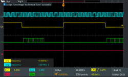
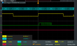
Attached to the post the screenshots of the I2S signals and the !PDN pin. They look good to me, it is a 48khz / 64FS stream, with 32bit per slot and 16bit of useful data. it is a left-right test signal, I also tried to connect another hat with other type of I2S amplifier, they play fine.
This is the sequence I applied, using some python scripts
1) Toggle !PDN pin to low
2) sleep 5 seconds
3) Toggle !PDN pin to high
4) sleep 1 second
5) Register dump#1
4) Start playback, I2S signals active
5) Init sequence
6) sleep 1 second
7) Register dump #2
This is the init sequence
bus.write_byte_data(0x4c, 0x00, 0x00)
bus.write_byte_data(0x4c, 0x7f, 0x00)
bus.write_byte_data(0x4c, 0x4c, 0x30)
bus.write_byte_data(0x4c, 0x03, 0x03)
sleep(0.005)
bus.write_byte_data(0x4c, 0x78, 0x80)
This is dump#1
0x39: CLKDET_STATUS: 0x00
0x68: POWER_STATE: 0x00
0x69: AUTOMUTE_STATE: 0x00
0x70: CHAN_FAULT: 0x00
0x71: GLOBAL_FAULT1: 0x00
0x72: GLOBAL_FAULT2: 0x00
0x73: WARNING: 0x00
0x28: SIG_CH_CTRL: 0x00
0x37: FS_MON: 0x00
0x38: BCK_MON: 0x40
0x5e: PVDD_ADC: 0x00
0x67: DIE_ID: 0x95
This is dump#2
0x39: CLKDET_STATUS: 0x00
0x68: POWER_STATE: 0x01
0x69: AUTOMUTE_STATE: 0x00
0x70: CHAN_FAULT: 0x01
0x71: GLOBAL_FAULT1: 0x00
0x72: GLOBAL_FAULT2: 0x00
0x73: WARNING: 0x01
0x28: SIG_CH_CTRL: 0x00
0x37: FS_MON: 0x00
0x38: BCK_MON: 0x40
0x5e: PVDD_ADC: 0x78
0x67: DIE_ID: 0x95
last dump shows several difference from the "normal operation"reported by lutkeveld
I still don't understand if the issue is caused by the OCP reported on right channel or by something else.
I will remove the output filters and try again if I get something new, I did't use the 10uH coils of the reference design, but some ferrite beads (in the datasheet it was fine for reduced output power). I did't change any settings to take this into account, can this be the root cause?
I noticed the small reference PCB shared by lutkeveld is using ferrite beads too, but he has 1nF capacitors and I have 680nF, as per reference design.
Attachments
I finally have my PCBs playing audio... my assumption about the capacitor was correct, removing them OCP was gone, and register had right values, using very same sequence.
I put back other capacitors (1nF), no OCP and audio playing fine.
Thanks again for your support!
I put back other capacitors (1nF), no OCP and audio playing fine.
Thanks again for your support!
I was just going to reply that, but you already found it yourself 🙂
680nF is for the LC output filter, the recommended value for FB based filters is 1 or 2 nF
The upside of FB is of course size/price, but the quiescent current is almost double and filtering (audio and electromagnetic) is also much worse. But in some cases the trade-off is okay.
680nF is for the LC output filter, the recommended value for FB based filters is 1 or 2 nF
The upside of FB is of course size/price, but the quiescent current is almost double and filtering (audio and electromagnetic) is also much worse. But in some cases the trade-off is okay.
See for example figure 5 in TI SLOA145 : http://www.ti.com/lit/an/sloa145/sloa145.pdf
Or look at other reference designs that actually use FB filters instead of LC, like the TAS5805M EVM
Or look at other reference designs that actually use FB filters instead of LC, like the TAS5805M EVM
Thanks!
I think TI should give a better review of their datasheets, I've spotted several typos and missing details on the TAS5825M one. Furthermore, spreading information on several documents can be confusing. I usually use datasheets as the "source of truth", but apparently it is not enough.
In my case using ferrite beads was a design choice to minimize cost and PCB area. Increase on THD will not be so severe to be audible, increase on idle consumption will be negligible, especially turning off the amplifier when playback is not active.
Is site down?

Who? Us or them? The link works for me.
Also no need to re-post. As a newbie your posts need approval before appearing 🙂
Ups.. Sorry.. Very strange. Unfortunately I have access to aurel32`s repo only with VPN addon in my browser! The git (as command) do not have this access. Can someone clone this repo and put the zip archive here?
Thank you for sharing this. Great work.
One Question: Did you made a dtoverlay for the RPi like justboom or hifiberry?
Hello,
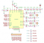
Similar to the project presented here, I was interested for an 'updated' TAS5828M implementation.
I have received the draft design, from a hired free-lance, to use TAS5828M and I would like to get your opinion before sending it for manufacturing:
Mostly based on https://github.com/tonyp7/TAS5806M-Audio-Amplifier


Looking forward for your feedback,
Similar to the project presented here, I was interested for an 'updated' TAS5828M implementation.
I have received the draft design, from a hired free-lance, to use TAS5828M and I would like to get your opinion before sending it for manufacturing:
Mostly based on https://github.com/tonyp7/TAS5806M-Audio-Amplifier
Looking forward for your feedback,
Not too bad actually. For reference have a look at the EVM: https://www.ti.com/lit/ug/slau860a/slau860a.pdf
I would move the middle bootstrap caps a bit more inward, like on the EVM:

Same for the output filter caps, position them a bit more in line between the inductor and output terminal like on the EVM:

And flip the power decoupling capacitors so that their ground side connects directly to the middle exposed pad instead of using a via.
This goes for all GND pads of the TAS, just connect them directly to the middle pad.
Nowadays, 4 layer is barely more expensive than 2 layer. So while it's possible to route the power underneath the inductors like is done now, I personally would just opt for a 4 layer and use a dedicated power layer.
I would move the middle bootstrap caps a bit more inward, like on the EVM:
Same for the output filter caps, position them a bit more in line between the inductor and output terminal like on the EVM:
And flip the power decoupling capacitors so that their ground side connects directly to the middle exposed pad instead of using a via.
This goes for all GND pads of the TAS, just connect them directly to the middle pad.
Nowadays, 4 layer is barely more expensive than 2 layer. So while it's possible to route the power underneath the inductors like is done now, I personally would just opt for a 4 layer and use a dedicated power layer.
Hello,
I have uploaded all the files here including the Altium project files:
https://github.com/Glider95/TAS5828M--Audio-amplifier.
I am not the one who created the design (I have hired a freelancer) so I will try to implement @lutkeveld proposition later !
I have uploaded all the files here including the Altium project files:
https://github.com/Glider95/TAS5828M--Audio-amplifier.
I am not the one who created the design (I have hired a freelancer) so I will try to implement @lutkeveld proposition later !
Last edited:
- Home
- Amplifiers
- Class D
- TAS5825M based amp