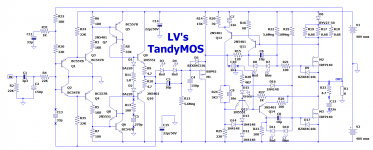
It has no diff-pair input, no DC-servo (yet its DC offset is negligible), no complementary output, no adjustments (yet its quiescent current is stable and deterministic), it uses ordinary vertical enhancement NMOS having a normal threshold voltage, yet it is free from the output swing limitations normally associated with such devices. The topology is half non-switching, half class AB and inverting.
In short: an oddity.
It is based on the Tandem topology, which has been evoked here: https://www.diyaudio.com/community/...here-is-the-legacy-thread.387391/post-7059293
I have already described a Tandem-based amplifier: https://www.diyaudio.com/community/threads/tandem-based-amplifiers.388400/post-7074596 but it was essentially a showcase and a test-bed for the concept: the VAS was simply an operational amplifier, thus limiting the power to 10~20W, since HV opamps like the LM143 have mostly disappeared.
It could certainly be used though, and for domestic applications the power is ample enough.
However, DIYaudio members prefer something more substantial, and here it is: the front-end is now completely discrete, meaning the rail voltages can be as high as necessary.


The tandem topology has been adapted to MOS (mostly by Minek), and a clever trick overcomes the limitation caused by the threshold voltages.
The Vth-erasers are simply voltage-memory circuits inserted in series with the gate, to reduce or cancel the threshold voltage, changing the MOS into a zero-threshold type. The circuits themselves are extremely simple: a capacitor paralleled with a shunt-regulating device (LEDs in this case), and fed by a large value resistor.
In principle, the concept could be used in any other amplifier (and I have done it in the Circlomos), but with "normal" amplifiers there is a difficulty: the voltage needs to be very stable and accurate because it will influence the quiescent current.
By contrast, the Tandem stage has its quiescent current tightly controlled by a feedback loop, and the only effect of a non-optimal voltage is a tiny reduction of the output swing: not a big deal.
Unfortunately, MOS transistors do not shine in the tandem topology: with the original semi's line-up, I couldn't bring the THD below 0.85%, even with the tweaks at their optimum. M1 was a IRFD9120 (which explains the 4-pin socket).
With a BSP92 or even a BJT (2N5401), this was reduced to 0.25%.
Better, but a far cry from the BJT tandem: 0.004%.
The inferiority of the MOS version is probably down to the numerous parameter mismatches: a BJT is characterized by the BE PN junction, which becomes a NP junction for the correction transistor, and there is relatively little wiggle room outside of the fundamental exponential V-to-I relationship.
With MOS transistors of different sizes and polarirty, things become much more complicated. It is probably possible to improve the matters by hand-picking transistors having nicely scaled parameters, but I didn't go that far.
Anyway, in this case it does not matter very much, even with the worst-case 0.85%.
The front-end has a huge open-loop gain (almost half a million), and a relatively mediocre THD: between 1.5 and 2%. This THD will dominate, because there is no definite addition rule for THD: in theory, perfectly coherent distortions could add arithmetically, or anti-coherent distortions could even cancel one another (error-correction situation), but such situations only happen when they are deliberately planned for.
In normal cases, you are somewhere in-between. When lots of random processing blocks are cascaded, the end result will tend towards the root of the sum of squares, but in simpler cases, it could be anything but will generally be close to the largest value, in this case ~1.7%.
When the loop is closed, this value will be reduced by the loop-gain, which is substantial, and results in a final THD figure of ~3ppm, thus quite good, but not enough to qualify as a "super-amplifier".
About the front-end:
It could raise eyebrows: it is based on a raw, undegenerated diamond structure, which looks risky and brutal. Howevever, because of the GNFB, Q3/Q4 and Q7/Q8 are forced to have the same current, and the rest of inequalities only have a minor effect.
In practice, it works like a charm: I picked the transistors at random from the drawer, didn't attempt any matching of any sort, yet it worked perfectly.
The schematic has oddities that deserve explanations:
C4 and C5 compensate the negative capacitance generated by M1.
The feedback network is split in two sections: R31/R32 and R30/R4. With a single network, the feedback resistor would need to be quite large if the input impedance has a civilized value, like 10K.
With a large resistor, stray capacitances can have unpredictable effects, which are neatly avoided here.
D15 generates a voltage transmitted by D16 to the "memory" circuit, precharging it.
In cold start conditions, with a large signal applied, M3 is unable to conduct sufficiently to satisfy the FB loop and M1 becomes saturated, leading to an overcurrent in D7 and D8 and the protection diode D9..
M3 is not controlled directly by the signal: it is slave to the upper transistor, via Q12, Q13 and Q14, and if M2 is off, M1 can conduct as much as wants it cannot make M3 conduct if the Vth eraser is not ready.
The precharge voltage is unsufficient to make M3 conduct, but it can as soon as an additional stimulus is added
This is the circuit with a BJT instead of M1: the Vth eraser has been shorted:

This is the 10kHz trangle response, just under the clipping:

The same, clipping:

Squarewave response, also 10kHz:

The measurements were made on this circuit:

I also include a simulation file, but it is not up to date: simulation and reality diverge significantly with this type of circuit
In short: an oddity.
It is based on the Tandem topology, which has been evoked here: https://www.diyaudio.com/community/...here-is-the-legacy-thread.387391/post-7059293
I have already described a Tandem-based amplifier: https://www.diyaudio.com/community/threads/tandem-based-amplifiers.388400/post-7074596 but it was essentially a showcase and a test-bed for the concept: the VAS was simply an operational amplifier, thus limiting the power to 10~20W, since HV opamps like the LM143 have mostly disappeared.
It could certainly be used though, and for domestic applications the power is ample enough.
However, DIYaudio members prefer something more substantial, and here it is: the front-end is now completely discrete, meaning the rail voltages can be as high as necessary.
The tandem topology has been adapted to MOS (mostly by Minek), and a clever trick overcomes the limitation caused by the threshold voltages.
The Vth-erasers are simply voltage-memory circuits inserted in series with the gate, to reduce or cancel the threshold voltage, changing the MOS into a zero-threshold type. The circuits themselves are extremely simple: a capacitor paralleled with a shunt-regulating device (LEDs in this case), and fed by a large value resistor.
In principle, the concept could be used in any other amplifier (and I have done it in the Circlomos), but with "normal" amplifiers there is a difficulty: the voltage needs to be very stable and accurate because it will influence the quiescent current.
By contrast, the Tandem stage has its quiescent current tightly controlled by a feedback loop, and the only effect of a non-optimal voltage is a tiny reduction of the output swing: not a big deal.
Unfortunately, MOS transistors do not shine in the tandem topology: with the original semi's line-up, I couldn't bring the THD below 0.85%, even with the tweaks at their optimum. M1 was a IRFD9120 (which explains the 4-pin socket).
With a BSP92 or even a BJT (2N5401), this was reduced to 0.25%.
Better, but a far cry from the BJT tandem: 0.004%.
The inferiority of the MOS version is probably down to the numerous parameter mismatches: a BJT is characterized by the BE PN junction, which becomes a NP junction for the correction transistor, and there is relatively little wiggle room outside of the fundamental exponential V-to-I relationship.
With MOS transistors of different sizes and polarirty, things become much more complicated. It is probably possible to improve the matters by hand-picking transistors having nicely scaled parameters, but I didn't go that far.
Anyway, in this case it does not matter very much, even with the worst-case 0.85%.
The front-end has a huge open-loop gain (almost half a million), and a relatively mediocre THD: between 1.5 and 2%. This THD will dominate, because there is no definite addition rule for THD: in theory, perfectly coherent distortions could add arithmetically, or anti-coherent distortions could even cancel one another (error-correction situation), but such situations only happen when they are deliberately planned for.
In normal cases, you are somewhere in-between. When lots of random processing blocks are cascaded, the end result will tend towards the root of the sum of squares, but in simpler cases, it could be anything but will generally be close to the largest value, in this case ~1.7%.
When the loop is closed, this value will be reduced by the loop-gain, which is substantial, and results in a final THD figure of ~3ppm, thus quite good, but not enough to qualify as a "super-amplifier".
About the front-end:
It could raise eyebrows: it is based on a raw, undegenerated diamond structure, which looks risky and brutal. Howevever, because of the GNFB, Q3/Q4 and Q7/Q8 are forced to have the same current, and the rest of inequalities only have a minor effect.
In practice, it works like a charm: I picked the transistors at random from the drawer, didn't attempt any matching of any sort, yet it worked perfectly.
The schematic has oddities that deserve explanations:
C4 and C5 compensate the negative capacitance generated by M1.
The feedback network is split in two sections: R31/R32 and R30/R4. With a single network, the feedback resistor would need to be quite large if the input impedance has a civilized value, like 10K.
With a large resistor, stray capacitances can have unpredictable effects, which are neatly avoided here.
D15 generates a voltage transmitted by D16 to the "memory" circuit, precharging it.
In cold start conditions, with a large signal applied, M3 is unable to conduct sufficiently to satisfy the FB loop and M1 becomes saturated, leading to an overcurrent in D7 and D8 and the protection diode D9..
M3 is not controlled directly by the signal: it is slave to the upper transistor, via Q12, Q13 and Q14, and if M2 is off, M1 can conduct as much as wants it cannot make M3 conduct if the Vth eraser is not ready.
The precharge voltage is unsufficient to make M3 conduct, but it can as soon as an additional stimulus is added
This is the circuit with a BJT instead of M1: the Vth eraser has been shorted:
This is the 10kHz trangle response, just under the clipping:
The same, clipping:
Squarewave response, also 10kHz:
The measurements were made on this circuit:
I also include a simulation file, but it is not up to date: simulation and reality diverge significantly with this type of circuit
Attachments
Last edited:

At last some one doing something different I am still looking at your amplifier and so far I like what I see
Trev
Trev
Very nice bread-boarding!It has no diff-pair input, no DC-servo (yet its DC offset is negligible), no complementary output, no adjustments (yet its quiescent current is stable and deterministic), it uses ordinary vertical enhancement NMOS having a normal threshold voltage, yet it is free from the output swing limitations normally associated with such devices. The topology is half non-switching, half class AB and inverting.
In short: an oddity.
It is based on the Tandem topology, which has been evoked here: https://www.diyaudio.com/community/...here-is-the-legacy-thread.387391/post-7059293
I have already described a Tandem-based amplifier: https://www.diyaudio.com/community/threads/tandem-based-amplifiers.388400/post-7074596 but it was essentially a showcase and a test-bed for the concept: the VAS was simply an operational amplifier, thus limiting the power to 10~20W, since HV opamps like the LM143 have mostly disappeared.
It could certainly be used though, and for domestic applications the power is ample enough.
However, DIYaudio members prefer something more substantial, and here it is: the front-end is now completely discrete, meaning the rail voltages can be as high as necessary.
View attachment 1090462
View attachment 1090463
The tandem topology has been adapted to MOS (mostly by Minek), and a clever trick overcomes the limitation caused by the threshold voltages.
The Vth-erasers are simply voltage-memory circuits inserted in series with the gate, to reduce or cancel the threshold voltage, changing the MOS into a zero-threshold type. The circuits themselves are extremely simple: a capacitor paralleled with a shunt-regulating device (LEDs in this case), and fed by a large value resistor.
In principle, the concept could be used in any other amplifier (and I have done it in the Circlomos), but with "normal" amplifiers there is a difficulty: the voltage needs to be very stable and accurate because it will influence the quiescent current.
By contrast, the Tandem stage has its quiescent current tightly controlled by a feedback loop, and the only effect of a non-optimal voltage is a tiny reduction of the output swing: not a big deal.
Unfortunately, MOS transistors do not shine in the tandem topology: with the original semi's line-up, I couldn't bring the THD below 0.85%, even with the tweaks at their optimum. M1 was a IRFD9120 (which explains the 4-pin socket).
With a BSP92 or even a BJT (2N5401), this was reduced to 0.25%.
Better, but a far cry from the BJT tandem: 0.004%.
The inferiority of the MOS version is probably down to the numerous parameter mismatches: a BJT is characterized by the BE PN junction, which becomes a NP junction for the correction transistor, and there is relatively little wiggle room outside of the fundamental exponential V-to-I relationship.
With MOS transistors of different sizes and polarirty, things become much more complicated. It is probably possible to improve the matters by hand-picking transistors having nicely scaled parameters, but I didn't go that far.
Anyway, in this case it does not matter very much, even with the worst-case 0.85%.
The front-end has a huge open-loop gain (almost half a million), and a relatively mediocre THD: between 1.5 and 2%. This THD will dominate, because there is no definite addition rule for THD: in theory, perfectly coherent distortions could add arithmetically, or anti-coherent distortions could even cancel one another (error-correction situation), but such situations only happen when they are deliberately planned for.
In normal cases, you are somewhere in-between. When lots of random processing blocks are cascaded, the end result will tend towards the root of the sum of squares, but in simpler cases, it could be anything but will generally be close to the largest value, in this case ~1.7%.
When the loop is closed, this value will be reduced by the loop-gain, which is substantial, and results in a final THD figure of ~3ppm, thus quite good, but not enough to qualify as a "super-amplifier".
About the front-end:
It could raise eyebrows: it is based on a raw, undegenerated diamond structure, which looks risky. Howevever, because of the GNFB, Q3/Q4 and Q7/Q8 are forced to have the same current, and the rest of inequalities only have a minor effect.
In practice, it works like a charm: I picked the transistors at random from the drawer, didn't attempt any matching of any sort, yet it worked perfectly.
The schematic has oddities that deserve explanations:
C4 and C5 compensate the negative capacitance generated by M1.
The feedback network is split in two sections: R31/R32 and R30/R4. With a single network, the feedback resistor would need to be quite large if the input impedance has a civilized value, like 10K.
With a large resistor, stray capacitances can have unpredictable effects, which are neatly avoided here.
D15 generates a voltage transmitted by D16 to the "memory" circuit, precharging it.
In cold start conditions, with a large signal applied, M3 is unable to conduct sufficiently to satisfy the FB loop and M1 becomes saturated, leading to an overcurrent in D7 and D8 and the protection diode D9..
M3 is not controlled directly by the signal: it is slave to the upper transistor, via Q12, Q13 and Q14, and if M2 is off, M1 can conduct as much as wants it cannot make M3 conduct if the Vth eraser is not ready.
The precharge voltage is unsufficient to make M3 conduct, but it can as soon as an additional stimulus is added
This is the circuit with a BJT instead of M1: the Vth eraser has been shorted:
View attachment 1090464
This is the 10kHz trangle response, just under the clipping:
View attachment 1090465
The same, clipping:
View attachment 1090466
Squarewave response, also 10kHz:
View attachment 1090468
The measurements were made on this circuit:
View attachment 1090469
I also include a simulation file, but it is not up to date: simulation and reality diverge significantly with this type of circuit
The base currents of Q3Q4 are not enough for the correct operation of Q1Q2. It is necessary to provide additional current to the Q1Q2 connectors from the supply voltage rails.
C11 in the Feedback circuit gives an additional 10 degrees of phase shift at a frequency of 20Hz, what for?
C11 in the Feedback circuit gives an additional 10 degrees of phase shift at a frequency of 20Hz, what for?
Last edited:
half a million (457000 times - 40Гц ) it's in terms of power.The front-end has a huge open-loop gain (almost half a million),
by voltage:
gain open-loop 67600 times (96.6dB) at 40Hz
gain open-loop at 20kHz 2140 times (66.6dB)
with a simple adjustment, distortion can be reduced to 0.006% at 20 kHz.and relatively mediocre THD: 1.5 to 2%
Last edited:
I agree that the input stage q1, q2, q3, q4 can't possibly work as drawn in the first schematic in the first post. I didn't look at the .asc file so I don't know what was actually simulated. But it can't work because q3 and q4 can't get any base current except through reverse leakage through the base-emitter junctions of q1, q2.The base currents of Q3Q4 are not enough for the correct operation of Q1Q2. It is necessary to provide additional current to the Q1Q2 connectors from the supply voltage rails.
C11 in the Feedback circuit gives an additional 10 degrees of phase shift at a frequency of 20Hz, what for?
Yes, and they are quite ordinary: not specially good or bad, perfectly sufficient in non-demanding applications. I bought them by kilo's (literally!) 40 or 45years ago, and they remain in a pristine condition.Elvee did you ever measure those axial Philips capacitors?
I don't even bother to reform them, and in this application the leakage current needs to be minimal to keep the correct memory voltage.
I can measure a few of them, if you are interested
Pristine 🙂 Well when I went to school a long time ago teachers (some ex-Philips guys among them) wanted us to measure these (various series but all axial with the transparent blue sleeve) and axial ITT Marcon caps. After we measured these caps they mentioned the electrolyte in the blue axial caps to be Ranja 😀 They measured awful indeed. They were offered often in bulk at various electronic dump shops for many years and fellow DIYers warned each other for these. Philips later made excellent caps with solid aluminium, I still have large numbers in stock of these and regularly use these (128 SAL-RPM).
Ranja is a sugar sirup to make lemonade.
Ranja is a sugar sirup to make lemonade.
Last edited:
Yes, I had forgotten to draw the 22K resistors. The schematic has now been updated.The base currents of Q3Q4 are not enough for the correct operation of Q1Q2. It is necessary to provide additional current to the Q1Q2 connectors from the supply voltage rails.
C11 in the Feedback circuit gives an additional 10 degrees of phase shift at a frequency of 20Hz, what for?
C11 makes the DC gain equal to ~-2, without it the gain would be much larger and would multiply the input offset.
Correction: this is valid if C1 is omitted. With C1 in circuit, the DC gain becomes -1
Last edited:
between the bases of Q1/Q2 and the junction of the 4.7R resistors, the open-loop voltage gain at 1kHz is 450,000 timeshalf a million (457000 times - 40Гц ) it's in terms of power.
by voltage:
gain open-loop 67600 times (96.6dB) at 40Hz
gain open-loop at 20kHz 2140 times (66.6dB)
I would be very interested: can you elaborate?with a simple adjustment, distortion can be reduced to 0.006% at 20 kHz.
Yes, the schematic is now correctedI agree that the input stage q1, q2, q3, q4 can't possibly work as drawn in the first schematic in the first post. I didn't look at the .asc file so I don't know what was actually simulated. But it can't work because q3 and q4 can't get any base current except through reverse leakage through the base-emitter junctions of q1, q2.
between the bases of Q1/Q2 and the junction of the 4.7R resistors, the open-loop voltage gain at 1kHz is 450,000 times
If this were the case, then the gain open-loop at 1kHz would be 113dB, then I congratulated you on the transition to the superlinear region, but alas, in fact you have a gain open-loop of 91dB at 1kHz, which is also not small, but not enough for superlinearity.
yes, that is the correct value.Yes, I had forgotten to draw the 22K resistors.
Resistor R35 is connected to the supply voltage bus, not to the feedback circuit.
don't worry ...
Last edited:
all in turn, let's not rush....I would be very interested: can you elaborate?
The 22K is now connected where it should.If this were the case, then the gain open-loop at 1kHz would be 113dB, then I congratulated you on the transition to the superlinear region, but alas, in fact you have a gain open-loop of 91dB at 1kHz, which is also not small, but not enough for superlinearity.
In the sim below, you see the voltage at point A (same as output in fact) together with the input voltage times 100K, with an offset removed to remain in the picture. The pp voltage in A is 70V, and the input voltage 12.8Vpp, a ratio of 5.4, meaning the OL gain is 540,000.
That's a sim, in reality the gain is more like ~450,000.
The meaurement is made in transient analysis mode, to take large-signal effects into account (Early for example). The AC analysis would probably give an over-optimistic value
- Home
- Amplifiers
- Solid State
- TandyMOS is not your typical amplifier: