What does that bottom side pic say about u1, u2 & u3?Please use the marking reading for power supply PCB only to clear the marking for U1,U2 and u3.My power supply pcb have no marketing on it so I have used this image to clear it up
What does that pic say about u1, u2 and u3?
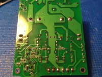
Where did that bottom side screen print come from?
It's a pity the sch for the PSU is nearly illegible. U1,2,3 are not drawn in a manner that helps explain.
Where did that bottom side screen print come from?
It's a pity the sch for the PSU is nearly illegible. U1,2,3 are not drawn in a manner that helps explain.
U1 PDTA114ET PNP with base resistors SOT-23 NXP RET SOT23 771-PDTA114ET215
U2 PDTC144ET NPN with base resistors SOT-23 NXP RET SOT24 771-PDTC144ET215
U3 PDTA115ET PNP with base resistors SOT-23 NXP RET SOT25 771-PDTA115ET215
U2 PDTC144ET NPN with base resistors SOT-23 NXP RET SOT24 771-PDTC144ET215
U3 PDTA115ET PNP with base resistors SOT-23 NXP RET SOT25 771-PDTA115ET215
Hi Andrew,
I don't know if this helps but here's my project page. This specific post explains what changes had to be done. My PCB is rev.1 not 2
It's in French so translate the page with Google.
Ampli NX Amp (version originale Hifisonix (Bonsai))
Thanks
Do
I don't know if this helps but here's my project page. This specific post explains what changes had to be done. My PCB is rev.1 not 2
It's in French so translate the page with Google.
Ampli NX Amp (version originale Hifisonix (Bonsai))
Thanks
Do
looks like u1 is a114 and not a144
I do wish Bonzai would confirm.
On my build, U1 is PDTA144ET.256. This was discussed in the thread somewhere I believe but not 100% sure. The speaker protection circuit has been working like a charm for the past almost two years.
Hope you get all you answers
Do
the pdf says a144, the BoM says both a144 and a114, the sch is illegible. But does state next to the device: PNP 10k which is the A114
The PCB does not say
The PCB does not say
Thanks for that.
Better quality sch that is legible.
It also shows the innards of the PDT transistors and confirms that U1 is 10k PNP = pdta114ET
Now stored in my Bonzai folder.
Better quality sch that is legible.
It also shows the innards of the PDT transistors and confirms that U1 is 10k PNP = pdta114ET
Now stored in my Bonzai folder.
The latest NX amplifier document is 2.09, November 2014. In cases where the schematic and BOM list different values for components, the BOM is usually more up to date.
Thanks for that.
Better quality sch that is legible.
It also shows the innards of the PDT transistors and confirms that U1 is 10k PNP = pdta114ET
Now stored in my Bonzai folder.
Have a look at post #871.
There was a reason Bonsai changed U1 to PDTA144ET
That change is unnecessary if a 27K resistor is added to the base connection of U1. All that was discussed back in the spring of 2014. If you already have a PDTA144ET then it's fine to use it but special ordering that part isn't necessary.
I had downloaded the latest pdf from Bonzai's site, I already had an older pdf from a previous download.The latest NX amplifier document is 2.09, November 2014. In cases where the schematic and BOM list different values for components, the BOM is usually more up to date.
That is where I came unstuck.
The PSU+Prot sch is not legible and the attached BoMs have anomalies, so I asked some questions.
It appears the Rb1 and R2 have been omitted from the sch and from the PCB.
except that the higher resistor value does not solve the potential overvoltage issue. That is mentioned in later posts.
For some reason the better solution of the added Rb1 was not put into the sch nor into the PCB. But it's an easy fix for those that keep a stock of 603 or 805 resistors.
Instead of 27k4, I had 22k and that gets the voltages and the currents down to very acceptable values even for a +-50Vdc supply.
One could even use a 1/4W 805 10k. With the lowest transistor resistor of ~8k the worst case current would be 51V/{10k+8k} = 2.83mA.
The two dissipations become 80mW & 64mW.
If one were using a 1/8W then Rb1 could be 18k for a worst case dissipation of 69mW (55.4% of rating).
Last edited:
I really just wanted to get you to that part of the discussion so you could see how things developed. I knew you would understand what was going on better than I could explain. I have the original boards so I had to cut in the resistors. Back then I didn't keep any SMD parts in stock so I used through hole resistors as can be seen in some of the pics I posted. I haven't seen the V2 boards.
It appears the Rb1 and R2 have been omitted from the sch and from the PCB.
Rb1 is something I added but Bonsai preferred to change U1 to PDTA144ET. The PC board was not changed to add Rb1 as you noted.
In the 2.09 document R2 is gone from the PC board and schematic but it remains in the BOM. I don't recall any mention of why it was removed but it doesn't appear to be critical either way.
I had downloaded the latest pdf from Bonzai's site, I already had an older pdf from a previous download.
That is where...
Andrew,
I'm glad to see you were finally able to get the PCB's and that you are building this amp. You've contributed greatly to DIY Audio over the years so I'm interested in your take on building and listening to this design.
I've been reading about several amp designs here since around 2008, i.e. DX Blame, various Apex, Nagy's Goldmund clone, Roender's FC-100, various Lazycat SSA's, Honeybadger, not to mention Pass designs like the F5 turbo. I chose the NX amp for a number of reasons:
1. Direct coupled and decent offset without a servo circuit.
2. Relatively low parts count and pretty much symmetrical schematic.
3. CFA design with wide bandwidth.
4. No "unobtanium" parts and PCB's available.
5. Excellent single .pdf document with everything in one place, so no need to sift through 1000's of forum pages to get all the key info.
The last 2 items are what really sealed the deal for me.
Bonsai, Thanks for all your work on this and for sharing!
- Home
- Amplifiers
- Solid State
- SX-Amp and NX-Amp