The board photo shows correct device placement. U1 is marked 03 as it should be.
Q3 is perhaps barely turned on since the drain is 51V. You do not have enough gate drive just as I didn't with R7=5.6K. When Q3 is fully turned on the drain should be near zero volts.
I'm not sure why D15 turns on immediately in your case. U1 is not fully turned on either with an output of 9.9V. Can you measure the voltage between U1 pins 1 and 2 (marked as 51.2 and 51V on your schematic)? It's almost as if there is some leakage current on your PC board, perhaps from contamination. Maybe cleaning with alcohol might help.
Hi Bill,
Checked again. 2mv across pins 1 and 2 on U1. I checked the part with voltages drained and there is no short across that part. I'm not sure why it reads that way. There are a few voltages that don't make sense. Where does the 3.19V come from between D2 and D4? 1.27V on the other side of D2 and 2.3V on the other side of D4. There's something happening that I don't understand.
I did clean the board with methanol. I did it again to make sure.
Is it possible for you to take some measurements of your board so I had something to compare to?
Thanks, Terry
Attachments
My board is in a chassis and I cannot get to the bottom side components without considerable disassembly. Here is what I measured from the accessible points on the top side of the card.
Q3 gate to gnd: 2.48V (with R7 = 20K)
junction of R27, R3, and R10 to gnd: 46.3V
V+ to gnd: 46.4V
Voltage across R27: 44.2V
Voltage across R3: 33V
Voltage across R10: 33V
With 2mV across pins 1 and 2 of U1, the device should be turned off. So the question is where does the 9.9V come from that you measure? With only 1.25V at the gate of Q3 your whole circuit should be off including D15 and all the power MOSFETs Q1 Q2 Q4 and Q5. Maybe measuring the voltage across resistors R27, R3, and R10 will provide a clue. With U1 off there should be no voltage at the junction of R27, R3, and R10.
The 3.19V you asked about is not DC and you need a scope to see the complex waveform. It comes from rectified AC voltage from the power transformer. D17 clamps the voltage and C2 filters it a bit but the ripple remaining is huge. R6 and C10 do most of the filtering so the gate of Q3 sees DC voltage. I think your circuit from the AC feed up to the gate of Q3 is functioning normally given the value of R7 at 5.6K. What I don't understand is why U1 outputs 9.9 Volts when it should be turned off. Gotta wonder if U1 is damaged...
Bonsai,
The power supply circuit has three LEDs that are powered from the V+and V- supply rails, about 50 volts. Resistors R21, R22, and R27 drop most of the voltage in setting the LED current to about 17mA. The resistors are 2.7K 1/2 watt but are dissipating around 0.75 watt in the application. I am using KOA resistors and their datasheet indicates a likely 85C temperature rise with the over-dissipation above rated power. If the internal ambient in the amplifier is 30C then the resistor will be at 115C and will likely fail early or discolor the PC board over time. When I get a chance I am going to change the resistors to 10K and see if the LED brightness is still acceptable. That will cut the power dissipation to about half the resistor power rating and keep operating temperatures well within maximum limits.
The power supply circuit has three LEDs that are powered from the V+and V- supply rails, about 50 volts. Resistors R21, R22, and R27 drop most of the voltage in setting the LED current to about 17mA. The resistors are 2.7K 1/2 watt but are dissipating around 0.75 watt in the application. I am using KOA resistors and their datasheet indicates a likely 85C temperature rise with the over-dissipation above rated power. If the internal ambient in the amplifier is 30C then the resistor will be at 115C and will likely fail early or discolor the PC board over time. When I get a chance I am going to change the resistors to 10K and see if the LED brightness is still acceptable. That will cut the power dissipation to about half the resistor power rating and keep operating temperatures well within maximum limits.
Well as for the 9.9V, if you subtract the 9.9 from the 44.4V across R27 you come very close to 33V you have across R3 and R10. I don't have any smd resistors. I will pull R7 and solder a through hole 20K there so I can try it.
Thanks, Terry
Thanks, Terry
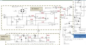
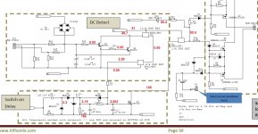
I've added some points about 2 months ago on debugging the PSU +Protectect board in the write up. Hopefully the points below will help you to isolate the problem:-
1. To verfiy that everything AFTER the 2N7002 (Q3) is working correctly, switch your meter to current mode and place the probes across GND and the DRAIN of Q3. The mosfet SSLR should turn ON (You are just shorting U1 input to ground). If they do not switch, you have an issue between the 2N7002 DRAIN and the mosfets. (Wire up an LED and a resistor between the SSLR output and V+ to monitor this)
2. To make sure your problem is not coming from the DC detect circuit, lift R1. If everyting works with R1 lifted, then your problem is with the switch ON delay circuit holding the gate of Q3 OFF, or loading it. You should fully test the switch on delay circuit before you re-solder R1 again.
3. You should get at least 2.5V on the gate of Q3, but preferably >3V. If not, check the component values and orientation in the turn on delay circuit. If this all looks ok, use Bill_P's fix (which I have adopted in the latest nx-Amp write up) and increase R7 from 5.6K to ~20k to get the >2.5V on the mosfet gate. Note that the 2N7002 should turn ON with Vgs of 3V (Id = 1mA) and with 2V will conduct typically 250uA Drain current. So, the 1.27 V you are reading is on the low side (but see my comment below).
4. If you do increase R7 to ~20k, make sure that the switch OFF time of the delay circuit is still fast enough to prevent any speaker thumps as the amp powers down.
Re Bill_P's comment about U1 output sitting at 9.9V, remember that on a 2N7002 (I'm looking that the FSC data sheet), it can conduct up to 250uA with only 1V on the gate - this is what you might be seeing - i.e. the device is just conducting a bit of current, and partially turning on. The cure is to make sure the gate is getting more drive.
http://www.fairchildsemi.com/ds/2N/2N7000.pdf
(Glad to hear you like the sound by the way!)
Last edited:
Hi Andrew,
As you probably know by now I don't have much knowledge about circuitry but I am trying to learn. I see how raising the resistance of R7 could raise the gate voltage of Q3. Wouldn't raising Q6 do the same? Also, I wonder if you had the same issue with the Jim's Audio PSU that you just built. Why do you think these values are so different from your original boards if he used the same Gerbers?
You said to make sure the protection still works properly. How do we test for that?
Thanks, Terry
no problem - We're all on a learning curve 😉
I've checked the Jims Audio boards (built 2 amp boards with R28/29 and R36/37 increased values) and tested the amps on an already built PSU. I am waiting for some additonal parts to complete asembly of the latest JA PCB. But, these boards are OK - they are exactly the same Gerbers I used - no difference. (The reason I bought a set was because I was worried that there were quality issues - there are none - the boards are ok!).
There are three factors playing here wrt the delay circuit - which is where some builders have experienced problems:-
1. AC detect signal coming in via C3 must be at the right level
3. Loading of R1
2. 2N7003 gate threshold level
If the AC detect signal is low due to lower seconday voltages, you will not get enough drive to the gate and this can lead to the delay circuit not turning on correctly. Ideally you want a solid signal coming in here that gives 3V or more on the gate. This will ensure the 2N7002 is solidly turned ON when AC is present. I see from your marked up schematic that the main rail voltages are at ~50V, so I assume the AC detect signal is ok.
Secondly, R7 in my design was set to 5.6k. Its low in order to provide a rapid discharge for C10 so the SSLR mosgets turn OFF before there are any speaker thumps during power down. If the mosfet gate threshold is high, this resistor can load the AC detect signal too much and only turn the mosfet on partially - which I think is what is happening because you say D15 is on - D15 will illuminate with Q3 partially turned ON.
On the third point, if you have amosfet with high threshold voltage (quite a normal spread for these devices), you will also experience switch on delay problems - and this of course is linked to the point above.
To fix 2 and 3 above, raise the value of R7 to ~20k.
For point 1 if your AC supply from the transformer secondary is less than 30V, you need to wire a second 1uF cap in parallel with C3.
I'l post up the test procedure for the PSU +Protect board - its straight from the nx-Amp document.
Last edited:
Here is the test procedure for the PSU +Protect board (you will need some crocodile clips to connect the battery, and a 1k resistor)
9. Once your PSU +Protection board is working (NB – don’t forget to reconnect R1 if you lifted it!) you need to do the following tests:-
a. Power up the board and let the SSLR engage. Switch your DVM to Ohms and measure across each of the SSLR’s. You should measure 0 Ohms (or at least <10milli Ohms if you have a very good meter with a low Ohms range). To double check that the gate drive is correct, switch your meter to V measure across D1 and D7 – you should measure ~12 V in each case
b. Next, take a 1.5 V AA or AAA cell (make sure they are new and measure the correct terminal voltage). Connect the cell across J10 pin 2 ( this is 0 V) and pins 1 and then 3. In both cases the SSLR should disengage. Note, it may take up to 1 second – this is perfectly ok with a 1.5V offset. Now turn the cell around and redo the test - the SSLR should disengage after about 1 second. This s the low voltage offset test.
c. Finally, use a 1k resistor and connect J10 pin 1 directly to V+ - the SSLR should disengage almost instantly; then connect it to V- and you should get the same result. Repeat the test on pin J10 pin 3 – you should get the same rapid disengage result on both V+ and V-
(Be careful not to short pin 2 of J10 to V+ or V- that’s why you should use the 1 K resistor).
This completes the testing of the PSU +Protection board.
Last edited:
Re Bill_P's comment about U1 output sitting at 9.9V, remember that on a 2N7002 (I'm looking that the FSC data sheet), it can conduct up to 250uA with only 1V on the gate - this is what you might be seeing - i.e. the device is just conducting a bit of current, and partially turning on. The cure is to make sure the gate is getting more drive.
Terry measured only 2 millivolts from U1 pin 1 to pin 2, indicating that there is no base current in U1 and Q3 is fully off. That's why I don't understand the presence of almost 10 volts at the output of U1.
The U1 device appears to be used well outside the manufacturer's specifications for input voltage and power dissipation. The collector to base voltage rating is being used right up to the limit as well. If R27 is raised to 10K as I suggested earlier, the reduction in U1 collector current should allow a lower base current to be used. Adding a base resistor or changing to a device with higher integrated resistors would then lower the power dissipation.
I'll post more on this later as I consider it further.
U1 consists of a PNP transistor with 10k Ohm base resistor and 10K Ohm base to emitter resistor. In the present circuit when Q3 is turned on the voltage across the U1 10K Ohm base resistor is nearly 50 volts. That yields a power dissipation of 0.25 Watt which corresponds to a temperature rise of 125C, yielding a junction temperature of 150C in a 25C ambient. The additional dissipation in the saturated collector to emitter junction is neglected in this calculation. 150C is the maximum allowable junction temperature before damage sets in. This is much too hot to be a good operating point for reliability.
If R27 is changed to 10K as discussed in a previous post, the total collector current in U1 is about 16mA. The device gain is at least 30 so if we design for a forced beta of 15 we need 1.1ma base current. Rounding off the base current loss in the 10K base to emitter resistor to 0.1mA, the base resistor current should be 1.2mA. Assuming a voltage drop of 45 volts in the total base resistance, 10K inside U1 plus a resistance added to the path, we need to add a 27k Ohm resistor from the drain of Q3 to the input of U1. That cuts the power in the U1 10K base resistor to 0.014 Watt.
Another option is to use a type PDTA144ET for U1. The 47K resistors that part contains would reduce the base current enough to control the power dissipation.
Bill,
None of the RETs are supposed to be partially on which is the condition you are describing. They should all switch on hard. For this to be the case, the 2N7002 needs a solid gate drive.
None of the RETs are supposed to be partially on which is the condition you are describing. They should all switch on hard. For this to be the case, the 2N7002 needs a solid gate drive.
Bill,
None of the RETs are supposed to be partially on which is the condition you are describing. They should all switch on hard. For this to be the case, the 2N7002 needs a solid gate drive.
No, I am assuming they are switched on fully saturated. The dissipation is almost all in the base resistor integrated into the SOT-23 package with the transistor.
Well I didn't have a 20k resistor so I just stuck an 18K resistor in R7. When I powered it up it blew D15. I took some measurements. Looks like I have worse problems now. I have attached a schematic. Perhaps I should just wait for Andrew to build his and see what he finds.
Blessings, Terry
Blessings, Terry
Attachments
OK I replaced D15 and this time it stayed lit. I comes on after about 5 seconds from power on. However, R27 is dissipating about 49V. Isn't that almost a full watt? Should I increase R27?
Thanks, Terry
Thanks, Terry
Yes, that's what I noted a while back. Try using 10K for R27. The voltages in your circuit look good otherwise. This is the first time Q3 has actually turned on in your power supply.
Thanks Bill,
Changed R27 to 10k. Dropped D15 to 1.8V and everything looks better. I ran all the tests from the build guide and all check out. The only things I'm not sure about is I see 49V on SC J7. I believe that connects to SC J1 on the amp boards which is the U1 FODM3012.
The other is that my rails are a hair over +-50V and C6 and C9 are 50V caps. I may need to go to 63V caps there.
Blessings, Terry
If you are testing the power supply board by itself, the voltage at SC seems ok. Also once the amplifier boards are connected and biased at 125 mA per output transistor, the V+ and V- should drop below 50 volts. What power transformer are you using?
You might want to consider changing R21 and R22 to 10K just as you did for R27. The issue is the same, over dissipation in the resistors. I made the change here and with 10K the LED's are plenty bright.
You might want to consider changing R21 and R22 to 10K just as you did for R27. The issue is the same, over dissipation in the resistors. I made the change here and with 10K the LED's are plenty bright.
Hi Bill,
Using an 400VA Antek Power Transformers An 4234 | eBay
I think I will R21 and R22 as well. Those LEDs ore very bright.
Thanks for all your help.
Blessings, Terry
Using an 400VA Antek Power Transformers An 4234 | eBay
I think I will R21 and R22 as well. Those LEDs ore very bright.
Thanks for all your help.
Blessings, Terry
- Home
- Amplifiers
- Solid State
- SX-Amp and NX-Amp