
Joel, you can get quite a spread in some of these parameters. Here is the ON data sheet for the BC560

They've only stated a typical value for 10 and 100uA and then for 2mA Ic, the shown spread is .55 through to 0.7V - a spread of 150mV. I typically see 10-20mV spreads, and on the ZTX851/951, I'm getting over 30mV.
On specs like this, manufacturers don't really focus on making them tight because its not something normally needed in the discrete world.
On the original sx-Amplifier released in 2012, I used very low value degeneration resistors of 15 Ohms and almost immediately builders ran into problems with the amplifiers sounding 'not right' or being unable to dial the output offset to 0 mV. Luckily I quickly realised the issue was if the base emitter voltages were not tightly matched, there would be serious problems - even 15mV of degeneration wasn't enough in some cases to counteract the Vbe differences of 20 or 30mV and in some cases much higher. In the sx-Amp, the solution was to either mandate matching Vbe's (not easy for constructors buying just enough parts to build an amp), or to increase the degeneration voltages in the diamond buffer stage so that the degeneration voltages swamped any Vbe differences, which is what I did, releasing an updated sx-Amp schematic and PCB within a month or so of the initial publication. The nx and kx2 amps use this same technique, and my commercial amps (Models 1701, 1707 and 1721) and there have been no further problems.
I expect you will see differences in Vbe between NPN and PNP as well. However, the designs with the high degenration voltages of 150mV means they won't affect performance markedly.
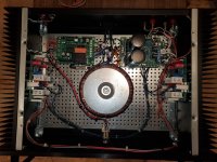
I'm curious what these heatsinks look like and how you determined what part to use. Would we be able to see inside this amp?Finally completed my SX rebuild in sheet aluminium case with porous ceramic heatsinks. It has the ripple eaters in too now. It sounds great.
Details in SS amps
View attachment 1118148
Yes I have posted before on this method for building cases and in combination with Amec thermasol porous ceramic parts.
https://www.diyaudio.com/community/...and-heatsinks-using-ceramic-heatsinks.380763/
https://www.diyaudio.com/community/...ing-internal-porous-ceramic-heatsinks.393139/
https://www.diyaudio.com/community/...and-heatsinks-using-ceramic-heatsinks.380763/
https://www.diyaudio.com/community/...ing-internal-porous-ceramic-heatsinks.393139/
Thanks. It looks like you can really decrease the overall enclosure size with those ceramic heat sinks. I'm trying to decide on a plan for an enclosure and it was really helpful to see how you have things laid out inside.
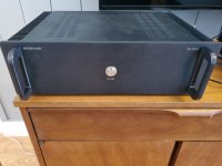
What is the jack that is on the left side of the front face?
What is the jack that is on the left side of the front face?
This was an experiment to see if what had worked with a dissipation of 30W could be pushed to 120W. I tried a number of layouts for different shapes and sizes, settling on this one as I like the overall form. Of course reducing the size of the amplifier and having the heatsinks internal means the heat has to escape mostly by updraft through the case. The inside of the amplifier does not get unduly warm -in the low to mid 40s C.
The jack is a good quality 4pin DIN for headphones. From the transformer dual secondaries, the amp is dual mono so the headphone channels are separate. There is a switch on the back and load/step down for the phones so I don't have to run two class A amps all the time just to listen on headphones for a bit.
The jack is a good quality 4pin DIN for headphones. From the transformer dual secondaries, the amp is dual mono so the headphone channels are separate. There is a switch on the back and load/step down for the phones so I don't have to run two class A amps all the time just to listen on headphones for a bit.
I'm in the process of starting up one channel of a new Ovation NX.
I have 700mv of DC Offset at full pot adjustment
All readings good until I got to measuring the DC offset.
R32 and R33 have 1.08V across them
Q8 is 547B, Q10 is 557B, Q9 is 546B and Q11 is 556B
Any suggestions?
I have 700mv of DC Offset at full pot adjustment
All readings good until I got to measuring the DC offset.
R32 and R33 have 1.08V across them
Q8 is 547B, Q10 is 557B, Q9 is 546B and Q11 is 556B
Any suggestions?
Across
R28=142mv R29=150mv
Q9 emitter wrt 0v=80mv and Q9 emitter wrt +out=825mv
Q11 emitter wrt 0v=208mv and Q11 emitter wrt +out=580mv
700mv across output
R28=142mv R29=150mv
Q9 emitter wrt 0v=80mv and Q9 emitter wrt +out=825mv
Q11 emitter wrt 0v=208mv and Q11 emitter wrt +out=580mv
700mv across output
Last edited:
Great, thank you Bonsai!
btw, I clipped on a 10K resistor across R1 for an R1 total of 5k ohms. The DC bias drops to 100ma.
Wondering about simply reducing R1 obtain correct DC bias
btw, I clipped on a 10K resistor across R1 for an R1 total of 5k ohms. The DC bias drops to 100ma.
Wondering about simply reducing R1 obtain correct DC bias
Hi Joel,
You should not have to change the value of R1 - under normal conditions it should provide ample offset adjustment. Seems there is some other issue here we should look into. Firstly, adjust R3 so that you are measuring 0V at the wiper. This will allow us to see what the actual DC readings are without interference from the offset adjust circuit.
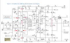
1. Can you confirm R36 and R37 = 150 Ohms and R28 and R29 = 120 Ohms.
2. Make sure R10 (10k) is in fact 10k - measure between the bases of Q8 and Q10 and 0V for this measurement.
3. If you have a gross Vbe mismatch all in the wrong directions on these devices, it could lead to offset issues on the sx and nx amplifiers. On the nx and sx Amplifiers, the output offset adjust was injected into the inverting input, so the required offset current is higher than is the case with my later designs that do this into the hi-z non-inverting input.
4. With that in mind, can you measure the Vbe across Q8 and Q10, Q9 and Q11 and then Q6 and Q7 as well; remeasure the voltage drops across R36, R37 and R28, R29
5. Also make sure the +-10V supplies (D4 and D3) are at 10V.
6. Can you confirm the volt drop across R24 and R25 is 82mV (do this measurement with no load connected to he output)
The voltage drops across
You should not have to change the value of R1 - under normal conditions it should provide ample offset adjustment. Seems there is some other issue here we should look into. Firstly, adjust R3 so that you are measuring 0V at the wiper. This will allow us to see what the actual DC readings are without interference from the offset adjust circuit.
1. Can you confirm R36 and R37 = 150 Ohms and R28 and R29 = 120 Ohms.
2. Make sure R10 (10k) is in fact 10k - measure between the bases of Q8 and Q10 and 0V for this measurement.
3. If you have a gross Vbe mismatch all in the wrong directions on these devices, it could lead to offset issues on the sx and nx amplifiers. On the nx and sx Amplifiers, the output offset adjust was injected into the inverting input, so the required offset current is higher than is the case with my later designs that do this into the hi-z non-inverting input.
4. With that in mind, can you measure the Vbe across Q8 and Q10, Q9 and Q11 and then Q6 and Q7 as well; remeasure the voltage drops across R36, R37 and R28, R29
5. Also make sure the +-10V supplies (D4 and D3) are at 10V.
6. Can you confirm the volt drop across R24 and R25 is 82mV (do this measurement with no load connected to he output)
The voltage drops across
Last edited:
0V on R3 wiper = 1.28V dc at the output with no load connected
1. R36 and R37 = 150 ohms R28 and R29 - 120ohms
2. R10 = 10K
3&4. Q8 = ..608V Q10 = .590V --- Q9 = .601V Q11 = .443V
5. D4 = 10.26V D3 = 10.23V
6. R24/R25 = 78mv across them ---- R26/R27 = 81mv across them
Adjusting bias is slightly jumpy- as I'm increasing it goes down a little before it starts increasing.
Q11 = .443V
That is not correct. I think you have a problem with that device. Can you change it out?
That is not correct. I think you have a problem with that device. Can you change it out?
Pardon me. I was on the wrong side of R28. Yes I get 0.44v from Q11 base through R28
I'm measuring VBE on the connecting resistors. I can't very easily connect to Transistor leads.
I changed out Q11 and then realized I was on wrong side of R28
I measured all vbe again- Q11=0.599 Q9= 0.614 Q10= 0.592 Q8= 0.618 - All looks good except DC at output is 1.3V
I'm measuring VBE on the connecting resistors. I can't very easily connect to Transistor leads.
I changed out Q11 and then realized I was on wrong side of R28
I measured all vbe again- Q11=0.599 Q9= 0.614 Q10= 0.592 Q8= 0.618 - All looks good except DC at output is 1.3V
Last edited:
Joel, have you shorted the input out? Please check that when measuring across R16 (power down with no load connected) you are measuring 540 Ohms and that R11 = 15 Ohms.
Strange that you have exactly the same problem on both boards.
Strange that you have exactly the same problem on both boards.
Beautiful build Joel! Trust you will have many hours of happy listening 👍👍👍
For NX R20 is 33 ohms in the schematic and on the regular BOM - circled in blue in the attachment
In the alternative BOM the value is 330 ohms
Is 330 ohms the new value? I installed 33 in the amp on post 2738 and no issue with bias adjust..
thanks!
close to wiring up another nx so thought I should ask.. A friend is taking my other one
In the alternative BOM the value is 330 ohms
Is 330 ohms the new value? I installed 33 in the amp on post 2738 and no issue with bias adjust..
thanks!
close to wiring up another nx so thought I should ask.. A friend is taking my other one
Attachments
Last edited:
- Home
- Amplifiers
- Solid State
- SX-Amp and NX-Amp