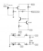
Here is a simple buffer circuit idea. You can use a BF244B or similar JFET. The Idss needs to be 10 mA or thereabouts. When I am back from vacation I will sim it - any volunteers for a PCB? Suggest an Alps RK27 pot or similar - a 24 step selector would b better, but they are not cheap ( Goldpoint start at about $150 I believe for a stereo attenuator).
Attachments
Last edited:
Buffer should have PSU onboard and volume pot onboard so that mounting requires only one hole on the front. Volume pot should keep pcb. If small enough this pcb could fit in any power amp chassis. PSU can have have some form of voltage dropping (preregulation) onboard so that power amp transformer can be used for buffer too. I think that opamp solution would be more than OK for this purpose. Such pcb could be universal and used in almost any power amp, not only nx.
There is many j-fet discrete buffers already so I think that opamp based one would be welcome addition.
Agree. You could just tap off the main supply screw terminals. I have just posted an idea up.
😱 You are very fast Andrew! Oh wait... I think you've done this before...Here is a simple buffer circuit.
 😀
😀OK - the extra boards I ordered when I ran short last time are on the FedEx delivery truck. I will have them in my hands late today, or if I miss a delivery, then tomorrow morning at the latest.
Yes, with cascoded front end, triple output stage and PSU ripple eaters.
I am getting 4ppm at 250W 20k and 7ppm at 360W (sims)
At 50W its about 500 ppb.
with straight Alexander comp, its about 13ppm at 360W 20k
I still have quite some investigation to do because I am trying some unusual comp methods (TPC, quasi TMC) and things are not as straight forward as with VFA's when you do this.
(BTW, I am getting about 70dB of PSRR at 10 Hz and around -120dB at 1kHz and it remains very good althe way out to HF (so >> 10kHz). The CFA PSRR thing is easy to fix IMV - I also suspect that this is where the real value of AFEC might be, so throw out the ripple eaters because they are big and bulky and use AFEC to get the PSRR up. When you are down at 10ppm distortion, AFEC does not add much value in terms of distortion reduction)
This project is still many months away because I am right in the middle of another big pre-amp project!
I was worrried there for a second whether you managed so low THD without it 😎 You figures are about in the ballpark I manage.
When you start experimenting youll notice how true the remarks I made about the compensation with CFAs in the Self thread is. Some in that thread just have absolutely no hands on experience with the topology and just recite whatever they read in books. It is perhaps possible to use 2 combining schemes, although some shunt will always be needed.
Link please? (for those of us who are always looking for new things to recite... 😀 ) Some of those threads are just incredibly long, and even doing searches can take a couple hours. Thanks....remarks I made about the compensation with CFAs in the Self thread is. Some in that thread just have absolutely no hands on experience with the topology ...
PMI,
There is a new thread that was just started to separate all of the cfa discussion from the Doug Self thread. The thread is listed this way: CFA Topology Audio Amplifiers
Hopefully we can stop some of the nonsense that some keep bringing up who just wont accept this topology no matter what because it seems Mr. Self does not endorse it! Though I will add that Bod Cordell seems very interested in this and adding information for his next box.
Re the buffer for the sx and nx: I just checked on Mouser. BF244 is being discontinued.
However, J111 (Idss 20mA minimum) is available and they have 47000 in stock. So this is the best choice.
You can also replace the 2 transistor current source with a single JFET as long as the current source JFET IDss falls well below the buffer FET Idss. So I would use the J111 for the buffer, and a J113 for the current source. Makes for a simpler design. I'll try to post up something a bit later.
this turns it into a copy of the B1 topology..............You can also replace the 2 transistor current source with a single JFET
This makes it different from the B1 and DCB1 where the Idss of the upper and lower devices match. i.e. the buffering jFET is biased to 100% of Idss.as long as the current source JFET IDss falls well below the buffer FET Idss. So I would use the J111 for the buffer, and a J113 for the current source. ....
Getting back to the nx power amp section...
Hi Bonsai
Can I increase the bias of output stage to get more class A power by changing the degeneration resistors from 0.33 ohms to 0.22 ohms and keek the indicated 40mv or so (instead of 26mv) across them without reducing the overall thermal stability of the output transistors?
Thanks
Fab
Hi Bonsai
Can I increase the bias of output stage to get more class A power by changing the degeneration resistors from 0.33 ohms to 0.22 ohms and keek the indicated 40mv or so (instead of 26mv) across them without reducing the overall thermal stability of the output transistors?
Thanks
Fab
Fab,
Yes you can increase the bias. I would leave the 0.33 ohms as is though for thermal stability reasons. You will be limited by the dissipation and the heat sink temperature. As a very rough guide, the highest your heat sink temp should go with moderate output power levels is 65 to 70 degrees Celsius. Make sure your heatsink can handle the extra power dissipation, and check that you do not have thermal runaway.
As the design currently stands, the output stage bias current is 125mA per pair, 250mA total.
Last edited:
Could small Mosfet be used instead of j-fet as buffer with two transistor CCS circuit in the post #181? Is there any mosfet buffer at all?
Fab,
Yes you can increase the bias. I would leave the 0.33 ohms as is though for thermal stability reasons. You will be limited by the dissipation and the heat sink temperature. As a very rough guide, the highest your heat sink temp should go with moderate output power levels is 65 to 70 degrees Celsius. Make sure your heatsink can handle the extra power dissipation, and check that you do not have thermal runaway.
As the design currently stands, the output stage bias current is 125mA per pair, 250mA total.
Bonsai
I thought that going further more over the 26mv drop into Re it would increase also THD furthermore...
Regarding the thermal stability, does Q3 needs to be as close as possible to the heatsink meaning having the pcb closest from to the heatsink?
From your initial response of this post you seem concerned about the loading of the VAS by the increase of bias in the output stage....
Also, can I use BD139/BD140 for the driver stage?
Thanks
Fab
Fab,
The nx-Amp is already biased at almost 2x the theoretical Iq value which for a 0.33 Ohm Rdegen resistor is c 78 mA ( ignoring re' and rbb' for the minute). I set the bias up at 125mA per pair and I did this because it gives another few hundred mW of class A. If you want to bias up using a lower Re of say 0.22 ohms that will also be ok just check for thermal stability - I have not tried 0.22 Ohms.
I am not fixated by the last few digits of distortion or setting the exact output bias current. I would just bias up the output so that you firstly have no cross over, and as much beyond this as you feel comfortable with because of thermal considerations and to maximize the mount of class A power.
Could small Mosfet be used instead of j-fet as buffer with two transistor CCS circuit in the post #181? Is there any mosfet buffer at all?
I have not tried this with a MOSFET. You would need to use one with a low Vgs threshold and input capacitance could be an issue. I will try to sim this when I get back home. I suspect noise will be worse than a JFET.
Regulated supply...
Any comments if we use independent regulated supplies for the front end of the NX amp?
That would be the ultimate ripple eaters ...or no ripple to eat at all...😛
Fab
Any comments if we use independent regulated supplies for the front end of the NX amp?
That would be the ultimate ripple eaters ...or no ripple to eat at all...😛
Fab
Last edited:
Bonsai,
Concerning your volume pot pcb for X-Altra Mini preamp, where did you find footprint for Alps Blue Velvet RK27 pot? This could be useful for PMI when designing input buffer pcb.
Concerning your volume pot pcb for X-Altra Mini preamp, where did you find footprint for Alps Blue Velvet RK27 pot? This could be useful for PMI when designing input buffer pcb.
Bonsai,
Concerning your volume pot pcb for X-Altra Mini preamp, where did you find footprint for Alps Blue Velvet RK27 pot? This could be useful for PMI when designing input buffer pcb.
Yes you could reg it with ripple eaters. The RC network off the zeners gives very good noise and ripple rejection though ...
"Also, can I use BD139/BD140 for the driver stage?"
IIRC the BD139/140 have Vce(max) = 80V.
I therefore would not use them for the nx-Amp where the total rail voltage is 100V.
IIRC the BD139/140 have Vce(max) = 80V.
I therefore would not use them for the nx-Amp where the total rail voltage is 100V.
"Also, can I use BD139/BD140 for the driver stage?"
IIRC the BD139/140 have Vce(max) = 80V.
I therefore would not use them for the nx-Amp where the total rail voltage is 100V.
Q9 and Q11 are 45v vce so I would not put +/- 50vdc for power rail😕
On my side I will use about +/- 40vdc.
Also, what is the final value for R34/R/35 since the schematics and bom call for 4k7 but the pcb marking states 10k😕
Thanks
Fab
- Home
- Amplifiers
- Solid State
- SX-Amp and NX-Amp