I did a model of the Stock amplifier. Found a few things about stability. First thing is the phase margin seems to dramatically shift depending on bias.
It really wants low bias about 18mA to 22mA per output device. Once it climbs to normal 30mA to 46mA the phase margins will swing almost 20 degrees.
The shift goes to a unstable margin.
Likely the main clue to why they can work fine then burst into oscillation. Aside from the fact square wave didnt look as bad as I thought.
But even in stock form it needed more compensation. In stock form the margin wasn't more than 20 to 22 degrees and that gets worse if bias climbs.
Here is look at square wave at 20 kHz
Not as bad as I thought it would be but has ringing and few overall ugly.
The more intense ringing on one side seems to be from negative DC offset
The amp is non inverting and should have positive offset.
Also noticed in the past any CFP amp doesnt like to much offset.
With more than 10mV the bottom or top rail will ring depending if the offset is
positive or negative.
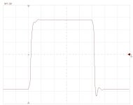
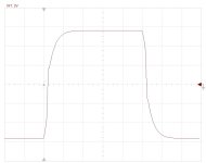
After a few simple mods and reducing the DC offset to be proper
Positive offset to less than 2mV. With just a slight increase in compensation values
The amp does rather fine and has a 45 degree or more stable phase margin
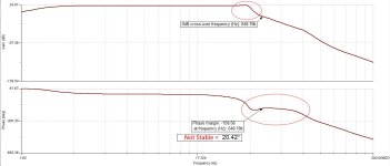
Here is AC analysis showing bandwidth and phase.
When bias is only 18mA to 20mA the phase margin is a unstable 25 to 27 degrees.
This graph shows when bias climbs to a still normal 30mA phase margin is even
worse at around 20 degrees.
As circled in red peaking near the end of the bandwidth. And near the 0 dB crossing
phase is still negative but is treading back upwards or more positive.
After slightly increasing the differential current from 1.5mA to 1.8mA
this was enough to get DC offset to be positive. And it was fine tuned
to be under 3mV by just using E96 or 1% resistor for the Differential resistor.
To further flatten the positive rise in phase and smooth the 0 dB crossing.
Compensation values just needed a slight increase in value.
Then it is also important to keep bias low around 18mA to 22mA
lower being better in this case.
C10 in the output area is horrible absolutely remove it
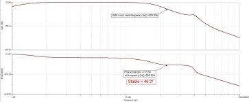
Here is the stock Model
Showing negative DC offset on output. Im sure this may vary
with real world devices and Rail voltage.
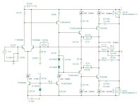
Here is simple mods to get positive DC offset
for a non inverting amplifier, and then changes to the CFP feedback
compensation and amplifier feedback compensation.
As noted above with these mods it is a Stable phase margin of 45 to 46 degrees

Was a easy fix. The real main problem with this amp is it needed only slightly more compensation.
And just a little more current for the differential.
The early problem, was the amplifier was still ok or marginally stable with likely low levels and normal music even with a poor 20 to 25 degree
phase margin. Problem is if it gets hot or if bias was set high from the start assuming 30 to 45mA is pretty normal for a amp.
Then the phase margin is very bad and will go into oscillation.
With low bias and added compensation, it likely wont be a little devil.
Another somewhat huge problem is C10 absolutely remove it, it causes a lot of phase margin issues
It really wants low bias about 18mA to 22mA per output device. Once it climbs to normal 30mA to 46mA the phase margins will swing almost 20 degrees.
The shift goes to a unstable margin.
Likely the main clue to why they can work fine then burst into oscillation. Aside from the fact square wave didnt look as bad as I thought.
But even in stock form it needed more compensation. In stock form the margin wasn't more than 20 to 22 degrees and that gets worse if bias climbs.
Here is look at square wave at 20 kHz
Not as bad as I thought it would be but has ringing and few overall ugly.
The more intense ringing on one side seems to be from negative DC offset
The amp is non inverting and should have positive offset.
Also noticed in the past any CFP amp doesnt like to much offset.
With more than 10mV the bottom or top rail will ring depending if the offset is
positive or negative.

After a few simple mods and reducing the DC offset to be proper
Positive offset to less than 2mV. With just a slight increase in compensation values
The amp does rather fine and has a 45 degree or more stable phase margin

Here is AC analysis showing bandwidth and phase.
When bias is only 18mA to 20mA the phase margin is a unstable 25 to 27 degrees.
This graph shows when bias climbs to a still normal 30mA phase margin is even
worse at around 20 degrees.
As circled in red peaking near the end of the bandwidth. And near the 0 dB crossing
phase is still negative but is treading back upwards or more positive.

After slightly increasing the differential current from 1.5mA to 1.8mA
this was enough to get DC offset to be positive. And it was fine tuned
to be under 3mV by just using E96 or 1% resistor for the Differential resistor.
To further flatten the positive rise in phase and smooth the 0 dB crossing.
Compensation values just needed a slight increase in value.
Then it is also important to keep bias low around 18mA to 22mA
lower being better in this case.
C10 in the output area is horrible absolutely remove it

Here is the stock Model
Showing negative DC offset on output. Im sure this may vary
with real world devices and Rail voltage.

Here is simple mods to get positive DC offset
for a non inverting amplifier, and then changes to the CFP feedback
compensation and amplifier feedback compensation.
As noted above with these mods it is a Stable phase margin of 45 to 46 degrees
Was a easy fix. The real main problem with this amp is it needed only slightly more compensation.
And just a little more current for the differential.
The early problem, was the amplifier was still ok or marginally stable with likely low levels and normal music even with a poor 20 to 25 degree
phase margin. Problem is if it gets hot or if bias was set high from the start assuming 30 to 45mA is pretty normal for a amp.
Then the phase margin is very bad and will go into oscillation.
With low bias and added compensation, it likely wont be a little devil.
Another somewhat huge problem is C10 absolutely remove it, it causes a lot of phase margin issues
It is a very bad construction that i absolutly recommend to get the fingers from.
The most important part is that there is no thermal control.
That means that if you have a success in adjusting an idle current in the output transistors they will overheat as soon as you play load music in it.
Normally there is a way to compare the voltage over the emitter resistors for the output transistors with the voltage over a sensor transistor that is mounted on the heat sink.That can be made in a number of different ways but they all have in common : the voltage over the output transistor emitter resistor is used to sense the current and compared with the voltage over a temperature sensitive element.
Then we have a low open loop gain that determines that the distortion is higher than usual in this cicuit.
You can simulate the open loop gain. Just set R2 to 0 and connect C2 to VG1 in the simulation.
Then you should add a 2k trim resistor between + and - feed with a 2k resistor from the mid point to C2.
With that trimmer you can adjust the output voltage from + max to - max. Do this only as a simulation for the open loop gain and phase. In the real world the amplifier will overheat.
Now you can test if the amplifier is stable in every voltage of a full output signal.
The normal way is to connect the drivers and output transistors as Darlingtons with emitter resistor from the output emitters to the output.
In that way you get faster output transisors with a possibility to thermal control and lower crossover distortion.
Played with this some more and found some issues. I notice that two bias diodes is a mistake because that means the driver Vbe cancels the diode thermal drift, which means the driver current is more or less constant, which means the OP bias does not thermal track. So you need 4 bias diodes, not 2, or a VBE multiplier.
Attached is a 3CFP circuit. It's tricky to stabilize but simulation claims pretty good THD. It eliminates the large CFP gain resistors and the 3 diodes keeps the two driver emitters voltage close so there is no reverse voltage problem and provides a ~class-B driver current boost on peaks. A single CFP gain network would do that too without any diodes but then there is no place to feed back bias. Theoretically, a CFP3 loses a diode drop on each side but it is barely visible in simulation.
It's fun to play with these things but I do have other things I should be doing.