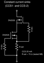
Hmm, that LND150 hint is nice! I might add a few to my next parts order, or I could just pick some DN2535 ouf of my stash (bigger brother of LND150, still only 1 pF Crss typical).
I'd need a bit more than 24 VDC PSU though, as the amp will need to swing more AC than this on the input of the OPS.
Thanks!
I'd need a bit more than 24 VDC PSU though, as the amp will need to swing more AC than this on the input of the OPS.
Thanks!
I mean - can't see any significant difference between these two, whichever you have in drawer ......
Yep the DN2540 will do nicely when much higher dissipation is needed.he needs more rail for full swing
I intended to use two DN2535/DN2540 for the CCS sections anyway, so to keep things easy and simple it makes sense to use a DN2535/DN2540 for the buffer, too. It's also nice that the DN will work fine at a lower voltage (unlike the STF3LN80K5). I'll have to change the biasing network a little bit to accommodate for the different Vgs, but that should be easy.
MB,
I build both tube and SS projects, so for me, this is a really neat one! Keep up the great work and good on you for doing something we haven't seen with a SIT.
Cheers,
Greg
I build both tube and SS projects, so for me, this is a really neat one! Keep up the great work and good on you for doing something we haven't seen with a SIT.
Cheers,
Greg
Hi Mbrennwa,
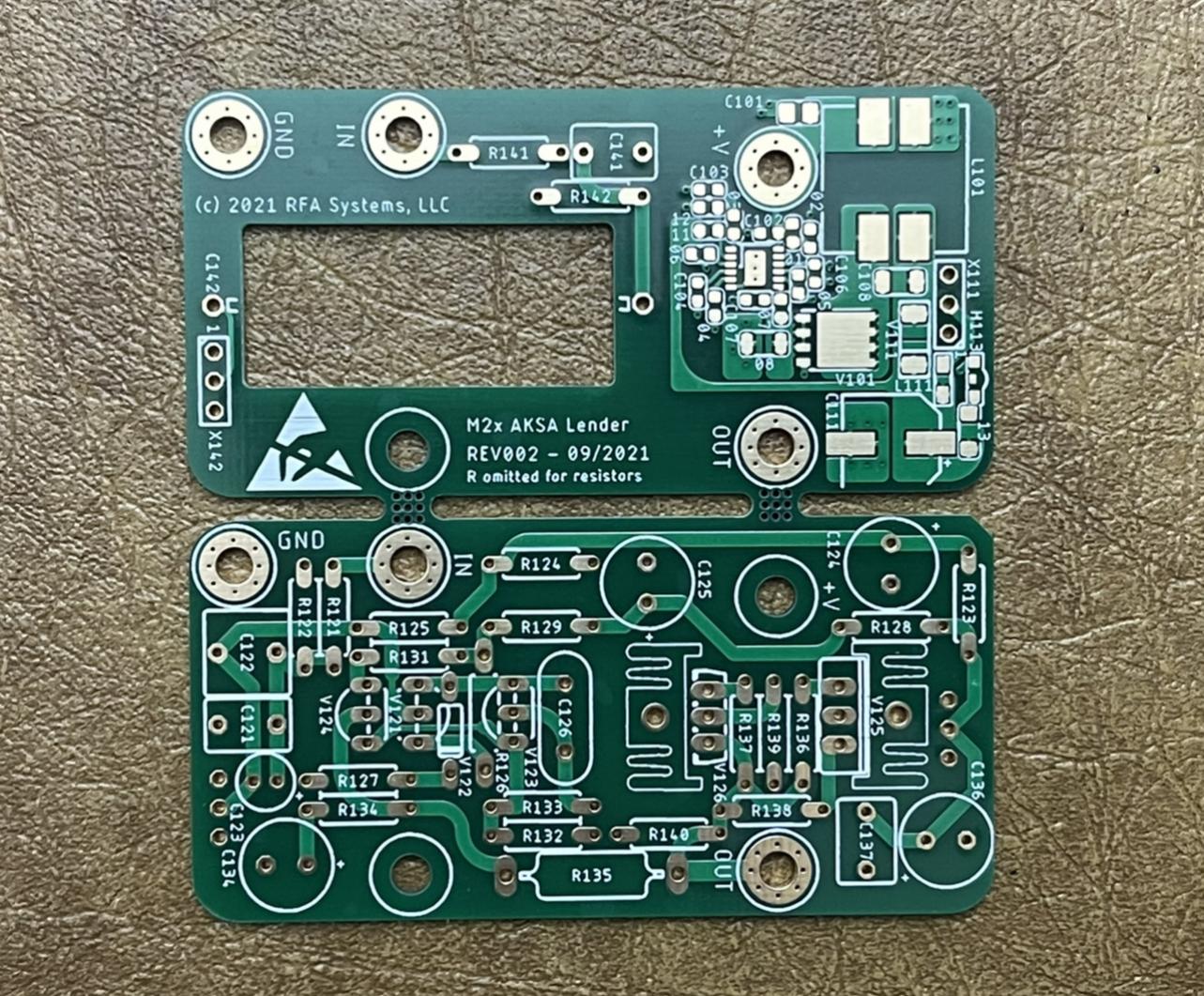
If you are interested, I can send you a set of Aksa Lender front end boards that I’ll be using on my SuSyLu. They will swing cleanly up to 50Vpp. The preamp itself is all TH but the 55v PSU DCDC booster is SMT.
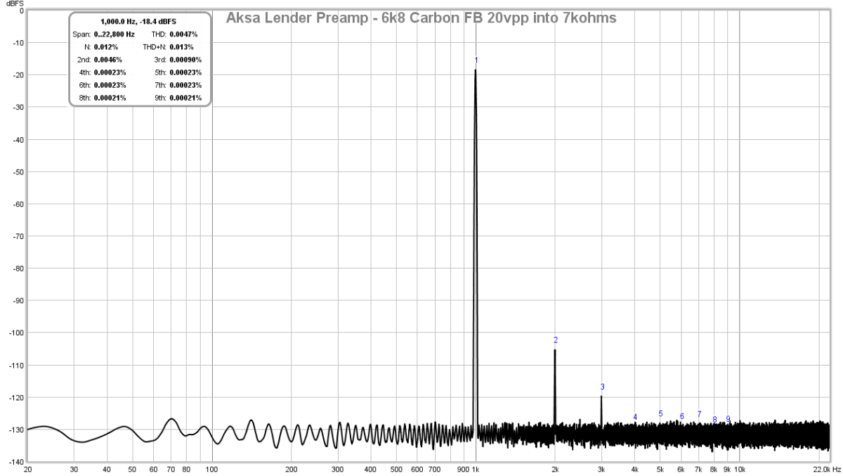
Here is typical FFT of output for 20Vpp:
If you are interested, I can send you a set of Aksa Lender front end boards that I’ll be using on my SuSyLu. They will swing cleanly up to 50Vpp. The preamp itself is all TH but the 55v PSU DCDC booster is SMT.
Here is typical FFT of output for 20Vpp:
Last edited:
That’s a nice modular solution for driving current amps and buffers. Wish I had built that instead of ASKA Lender preamp as a standalone.
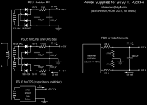
Here's some new and revised drafts (main circuit, PSU, CCS). Let me know what you think.
In the meantime I am waiting for feedback on my request for a custom made "double choke" load for the OPS...
In the meantime I am waiting for feedback on my request for a custom made "double choke" load for the OPS...
Attachments

The SIT gate needs to be at about -1 V to -2 V. The Vgs of the buffer FET (2DN2535) is about -1.3 V, so the buffer gate is close to 0 V. To allow some flexibility with the bias (-2 V to +2 V or so), a bipolar bias supply is needed. The buffer needs this anyway, so it's no extra complication.
Hold on, I believe ZM was right... I just built a mockup of the buffer and realised that my brain got the Vgs of the buffer FET backwards. The FET gate needs to be more negative than the source. The gate of the buffer FET gate therefore needs a more negative voltage than the gate of the SIT. The bias network can therefore use GND instead of the +40 V connection.
Also, when I was playing with my mockup, I blew the buffer FET (twice). I wasn't particularly careful, and I didn't have the protection Zener on the buffer FET. This may explain why the buffer FET went kaputt, but it also got me thinking: do I need a second Zener with reversed polarity on the buffer gate?
Also, when I was playing with my mockup, I blew the buffer FET (twice). I wasn't particularly careful, and I didn't have the protection Zener on the buffer FET. This may explain why the buffer FET went kaputt, but it also got me thinking: do I need a second Zener with reversed polarity on the buffer gate?
you need protective zeners for both SIT and mos
orientation for mos - just check what they say for max Ugs - is it positive or negative, orient zener accordingly
orientation for mos - just check what they say for max Ugs - is it positive or negative, orient zener accordingly
orientation for mos - just check what they say for max Ugs - is it positive or negative, orient zener accordingly
DN2535 datasheet says +/- 20 V. That's why I was thinking... TWO Zeners needed?
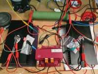
I matched some Tokins and then built a first mockup of the output stage. It's alive!
Biasing worked out as expected, and I managed to increase the rail voltage to 32 V and idle current to 2 x 3.3 A, where the heatsinks were still way cooler than in some of my previous amps.
Some first quick measurements are promising. I could get some very clean 50 W into 8 Ohm, and the onset of visible clipping on the scope was somewhere at maybe 90 W.
When I switched to music, the music peak voltage recorded on the scope was 30 V. The workshop dummy speaker made some nice music, so I lost interest in the measurements. It can go much louder than I'd ever want in a normal listening session.
Attachments

Maybe even to a negative bias only, i.e. the drain not yet charged/connected to Vb…7V5 or 8V2 will do
SITs and VFets are , at least to my knowledge, sensitive to excess negative gate voltage
for positive - newer read and never seen protection implemented
- I puzzle about this phenomenon, one of my SITs that has gate current already, does not like such a situation.
- does it leak from source to gate at that moment? Then I should insert a diode at the source. A SIC diode, for the Sick SIT🙁
- Home
- Amplifiers
- Pass Labs
- SuSy T. PuckFo