the same would happen on AD797 ?
If you reverse 7 and 4 the circuit will not work regardless of IC choice. .
Did you look at my version of the Super regulator for JLH69?
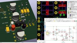
Good drawing - which program used ? Why did you add follower Q2 ?
OK, using the follower Q2 you want to free op amp output from
large current due to substantial current demand of the JLH amp.
I wonder why somebody wants to supply this simple power amp
with a complicated regulator.
JLH can be made with unregulated supply and still have low noise.
But this is off topic.
large current due to substantial current demand of the JLH amp.
I wonder why somebody wants to supply this simple power amp
with a complicated regulator.
JLH can be made with unregulated supply and still have low noise.
But this is off topic.
It's about low output impedance more than the noise. This Q2 trick could be useful i i wanted to do a lot of current with low beta pass transistor, but now with class a 2.5A and 5-7 volts offset, pass transistor gets really hot, it's beta rises and was around 120 to start with, is more like 150 now, so for mere 3.5max/150 = 23mA/2 = 12, say 15mA op amp bias to base current, the opamp handles the whole swing of base current on its own.
I decided to use two 3.6 zeners in series instead of 6.2 I'm using now.on forum about encryption i read it's giving much lower noise than a single higher voltage, and despite noise contribution formula, every little helps
I decided to use two 3.6 zeners in series instead of 6.2 I'm using now.on forum about encryption i read it's giving much lower noise than a single higher voltage, and despite noise contribution formula, every little helps
I do not think that these contribute to output noise.
Did you find the error in your negative regulator ?
Did you find the error in your negative regulator ?
Zener does contribute nise[/LEFT], as it is passing the DC to the base of pass transistor. It's contribution is maybe insignificant. due to the square law, but it's there.
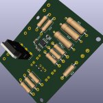
As for the error, not quite, as i have to order a whole new PCB, with pins 7 and 4 reversed to check it. I remember now i had the same problem in universal board and swapping solved the issue, probably i have done the same mistake in PCB project. It's too tight and small to repair now, and I've done the error to cramp everything, positive, negative rail, and JL,H on one small board.
It will be 3 separate boards now, with more space for resistors rn60d type and some ferrite beads on legs. More serviceable.
Last edited:
after consideration, i admit, that a serie of 3 difrent colours diodes may LOOK cool on PCB ..
i`m disconecting modules and doing the negative first as separate pcb.
with 3 LED in series instead od 6.2 zener, plus the fourth for CCS ref, arranged somehow, would look like this, funky..
i`m redoing the negative quarter, so schematic is not redrawn yet, just for a quick look:
with 3 LED in series instead od 6.2 zener, plus the fourth for CCS ref, arranged somehow, would look like this, funky..
i`m redoing the negative quarter, so schematic is not redrawn yet, just for a quick look:
Attachments
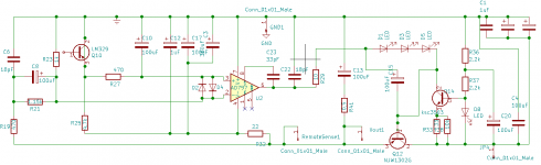
One connection missing - who can spot it? ;-)
Jan
it`s just a quick draft after revolving the opamp, i just started.
answer : CCS is not connected with base of pass transistor, and many others..
i need some more time, to make it also look good on schematic, i`m working on it like literally now.
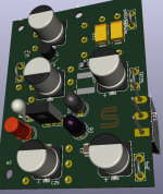
this might look like this now:
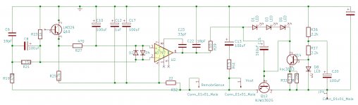
i enlarged the pitch of all resistors to facilitage Dale RN60 and Mills MRA-05. All caps on top, all very high temp, oscons 145 and tantalum polymer in less critical to AC paths, enough place for ferrite beads across CCS and voltage reference, all ceramics 1205 for comfortable soldering.
68 / 53 mm lenght/width
Attachments

Last edited:
What is the purpose of R32?
What input and output voltage are you planning for this unit?
Jan
What input and output voltage are you planning for this unit?
Jan
2.5A bias current for JLH1996,
Vout: +- 18V rails symmetrical
Vin: 2x24 (synchronous ultra low RDSon mosfets symmetrical LT4320, fed from 300VA 2x19VAC toroid)
Vin Ripple at 6A current draw (both channels driven) is of 20mV
R32 with C17 C12 is additional RC decoupling of the op amp and lm329
R41 is to fine-tune the square wave response.
Attachments
Last edited:
dang, when to think about it, just put a capacitance multiplier transistor with 1.2V offset, and at the cost of mere 3Watts and a transistor, i could have like uV ripple at the input , at the desired 2,5-3A draw per channel.
might get away with even 1V offset, and some smaller transistor TO-126 and a separate radiator. 3Watts is manegable.
might get away with even 1V offset, and some smaller transistor TO-126 and a separate radiator. 3Watts is manegable.
Last edited:
Sorry, schem in 2549 has more than one error.
can you please take a last look on my schematic against connection errors, before i start drawing traces ?
can you please also tell me, what you think about an additional 4.7k shunt resistor at the base of Q12 to ground ? Except from moving the bias point of the op amp, would it make a diffrence in reference to parasitic capacitances ?
Attachments
Last edited:
if i aim at 18,1V out, isn`t the 3xLED voltage drop too low for proper biasing of opamp ? 3x1,74 = 5,12V against 18.1. Should i add fourth LED and rise it to 7V?
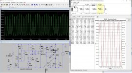
Also, according to LtSpice, in my circuit, the current spikes through 3xLED are 12-21mA with 360uF shunt, or 6-26mA with 100uF.
16mA average should get me low dynamic impedance on the diode. Is it wortwhile to put 360uF instead of 100uf to reduce the current spikes?
Also, according to LtSpice, in my circuit, the current spikes through 3xLED are 12-21mA with 360uF shunt, or 6-26mA with 100uF.
16mA average should get me low dynamic impedance on the diode. Is it wortwhile to put 360uF instead of 100uf to reduce the current spikes?
Last edited:
What is the purpose of R32?
What input and output voltage are you planning for this unit?
Jan
does this additional RC filter from R32 (22R) and 360uF electropolymer plus 100uF tantalum polymer hybrid plus 1uF C0G (or 1uF stacked PET),
at the power supply of AD797 plus the LM329
does R32 somehow worsenes the performance of this regulator? Why?
Stalin used to say : " trust, but control! Control, is the highest form of trust"
- Home
- The diyAudio Store
- Super Regulator