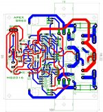
First layout try....
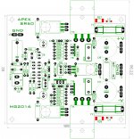
Board size : 92x100mm
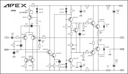
R4 on your schematic is 47k instead 180R...
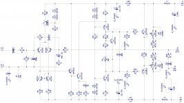
Thanks Miles. I found an another mistake....Here is corrected schematic
BC556 is PNP and pins reverted,,,
BC556 is PNP and pins reverted,,,
You have perfectly right....need to rework my copy...
Marc


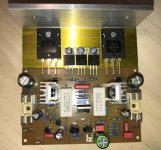
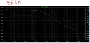
Hi, first test with SR60:
I have only made a few very short tests. Operating voltage is 50V, the current is 40mA, offset is 200mV, although I have matched the input transistors 😕
The poti does not change anything.
The sine at 1 kHz looks good. Unfortunately, I have no more time this weekend. I will continue next week.
It is exciting again with every new amplifier 🙂
regards Olaf
Attachments
Hi, first test with SR60:
I have only made a few very short tests. Operating voltage is 50V, the current is 40mA, offset is 200mV, although I have matched the input transistors 😕
The poti does not change anything.
The sine at 1 kHz looks good. Unfortunately, I have no more time this weekend. I will continue next week.
It is exciting again with every new amplifier 🙂
regards Olaf
Nice work, 100R pot is for BIAS you can add 220R pot to set DC offset.
Regards
Attachments
Hi
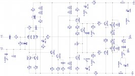
I was interested in this design and I input into LTSpice to see how well the SR60 does before I consider building one. I am getting oscillation depends on how the input driving condition. Attached is the simulation file, I use the transistor model file by Bob Cordell. I change a little bit by adding two extra output pairs. Also, I use BC547 instead of MPSA42 as I don't have the model.
I also run the THD test comparing with a typical Blameless amp, SR60 is about 15dB higher in 2nd and 3rd harmonics when I ran 1K, 5K, 10K and 20KHz at 1.4V input. I use 4ohm load, that's the reason I use 3 pairs of output transistors to avoid beta droop and lower crossover distortion. I run the transistor at 100mA per pair and use .22ohm emitter resistor.
Please tell me what I did wrong.
Thanks
Attachments
Go back to single output pair for the sim. Get that working first before you complicate it.
100mA through 0r22 Re gives 22mVre. This should be close to optimal ClassAB biasing.
What current does the sim say is flowing though the two VAS/TIS transistors?
No base stoppers on the output pair.
No Output Zobel.
What capacitance on the output caused the oscillation?
100mA through 0r22 Re gives 22mVre. This should be close to optimal ClassAB biasing.
What current does the sim say is flowing though the two VAS/TIS transistors?
No base stoppers on the output pair.
No Output Zobel.
What capacitance on the output caused the oscillation?

Go back to single output pair for the sim. Get that working first before you complicate it.
100mA through 0r22 Re gives 22mVre. This should be close to optimal ClassAB biasing.
What current does the sim say is flowing though the two VAS/TIS transistors?
No base stoppers on the output pair.
No Output Zobel.
What capacitance on the output caused the oscillation?
Same thing.
I attached exactly what you asked. I attached also the .asc for gain phase plot and the graph of the loop gain plot. Phase margin at loop gain=0dB is 0. At about -30dB( which is close to open loop gain=0dB), phase is -140deg. That's not stable.
There is no capacitance at the output. Base stop can only help particular for multiple pairs.
It make very little difference between 3 pairs of output transistors or one pair.
Attachments
note that the gain is less steep below 3MHz.
Then begins to steepen and has become very steep as it crosses 0dB @ ~4.4MHz.
This virtually guarantees oscillation.
You need to move the knee up in frequency to beyond 4.4MHz
That can be by using a faster device that is currently introducing just a bit too much phase delay, or by introducing a zero to flatten off the roll off in the 3 to 5MHz range.
The same device could be speeded up by changing it's Ic. fT is very dependant on Ic.
It may be that it is a good idea to give T7 a small heat sink. It gets very hot in my prototype.dc pot. added and some little cosmetic changes
regards Olaf
note that the gain is less steep below 3MHz.
Then begins to steepen and has become very steep as it crosses 0dB @ ~4.4MHz.
This virtually guarantees oscillation.
You need to move the knee up in frequency to beyond 4.4MHz
That can be by using a faster device that is currently introducing just a bit too much phase delay, or by introducing a zero to flatten off the roll off in the 3 to 5MHz range.
The same device could be speeded up by changing it's Ic. fT is very dependant on Ic.
It is obvious that in real life, this amp is stable.😕 This is a popular DIY amp. I tend to trust the real life result than the simulation.
It may be that it is a good idea to give T7 a small heat sink. It gets very hot in my prototype.
regards Olaf
Yes T7 work with 10mA and full rail voltage (over 100V in your prototype), it is 1W disipation. VAS transistors work with 12mA but half rail voltage that is 600mW.
Regards
Yes, I did not pay attention in the layout. But I'll include this in the layout before uploading the sprint file.
I'm curious about the sound when I've adjusted the offset.
I'm curious about the sound when I've adjusted the offset.
OLAF
Did you make scope measurement in the amplifier?
Could you please share it with us?
I also got oscillation in simulation and I believe 33nF + 22R is a big RC to put between amplifier inputs (personal opinion).
I remake the compensation arrangement and I add a predriver pairs in output stage. With these mods I got it stable in simulator and THD of 0.000267% with 55V rails.
sds/ronaldo
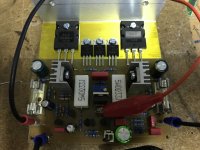
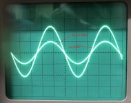
Hi, I have only measured the sine between input and output and that is clean (see picture). I do not think that the amplifier oscillates. Power consumption of the circuit and temperature of the transistors is as expected. Only the offset is a problem. With 470R instead of 180R the offset drops from -200mV to -120mV. At 1k I still have -100mV. There is something wrong. Can be, I still have a layout error or a transistor is not ok.
Otherwise no progress and tonight nothing more. 🙂
regards Olaf
Otherwise no progress and tonight nothing more. 🙂
regards Olaf
Olaf
Thank you about your answer. I could not see the picture.
I suppose there is big differences in your input devices. Can you match pairs?
I suppose it will resolve your problem.
I attached B285 file. It is a commercial product from 80's with this topology. Good sounding in my personal opinion. Also attached my version of SR60
SDS/Ronaldo
Attachments
Last edited:
- Home
- Amplifiers
- Solid State
- Studio Reference Amplifier