I have had brackets made which look pretty much like the previous offering
for the VFETs. They hold 4 x TO-3 power transistors and fit nicely on the
standard heat sink mounting pattern used on the sinks from the store.
for the VFETs. They hold 4 x TO-3 power transistors and fit nicely on the
standard heat sink mounting pattern used on the sinks from the store.
I do have four pairs of the Sony VFETS from circuitdiy 🙂. Would the two vfet diyaudio boards work with that version of the brackets or is this foreshadowing to part 3?
Jim
Jim
I do have four pairs of the Sony VFETS ...
Jim
That's all we need to build such amplifier , bracket isn't an issue , at all 🙄
.
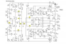
Help with Vfet bias voltage needed
I am building the two pair version using the Teabag Al boards and am testing them on the bench . No Vfets and IRF's have been installed.
Front end board bias and offset went smooth. I wanted to check the voltages before installing the output semis. Got 23 V + and - respectively for the IRF's between their gates on the PCB and ground. OK.
Problem is that the Vfet gate voltages dont seem to move much when pots P1 and P2 are turned.
I measured the voltage across the gate and source pins on the board.
Q4 Vgs -8.20 thru -10.12
Q6 Vgs +8.5 thru +10.40
If I measure between gate and ground the range is only between 8.4 and 8.7V
My Vfets are marked
Set1 - SJ28-9.1, 9.1 SK82- 8.5, 8.5
Set2 - SJ28-8.4, 8.4 SK82-7.6, 7.6
Zeners 3 and 4 are 15V as specified. Voltages directly across zeners about the same at 8.4-8.7V. Also, the second output board behaves the same way.
Puzzled? Advice appreciated.
Thanks. Nash
Attachments
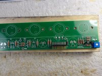
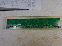
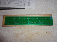
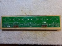
Post pics (in focus, will lit) of the boards, you never know what someone might spot.
Can you confirm R9/R10 resistance values and that the pots are indeed 5k? What about the pots' pinout?
The TL431 will try to maintain a voltage of typically 2.5V between the REF pin and its anode pin (ground). What voltage do you see there?
Can you confirm R9/R10 resistance values and that the pots are indeed 5k? What about the pots' pinout?
The TL431 will try to maintain a voltage of typically 2.5V between the REF pin and its anode pin (ground). What voltage do you see there?
check between VFet gate points and ground
without VFets in place , source points (out) is still floating , flapping in the breeze ....... not connected to anything
without VFets in place , source points (out) is still floating , flapping in the breeze ....... not connected to anything
check between VFet gate points and ground
...
I think he did.
...
Q4 Vgs -8.20 thru -10.12
Q6 Vgs +8.5 thru +10.40
If I measure between gate and ground the range is only between 8.4 and 8.7V
...
sorry .....
in that case , nothing left than TL431 orientation and resistors surrounding them
in that case , nothing left than TL431 orientation and resistors surrounding them
I concur. Tea-Bag's boards have the critters' case orientation silkscreened, so it's easy to check. Let's wait for the pics.
ZM rechecked one of the Vfets gate to ground- measured about 8,4v at one end of the pot, it stayed the same till around the middle position and then to 8.7v at the other end of the pot. Similar behavior on all 4 pots of both the boards. + and - polarity of voltage is correct.
RodeoDave R9 and R10 are 7.5k, measured when removed from bag and you can see it clearly in the attached pic.
Can someone help me understand how Z3 and Z4 work in this circuit? They are connected in the middle and then to the Vfet source pins, so does this mean that the Vfets have to be connected for them to work? I measured around 17v between the ends of Z3 and Z4 at the R1 R2 ends. Verified that the Mouser bag does say 15V for the zeners.
The TL431 critters are the A type.
You will notice that I have not connected the caps. However, just to be sure I connected C5, C6(47uf) on the one board. Same numbers.
Thanks. nash
Attachments
Without the caps it will oscillate. I would finish it up then run the tests again.
Also the 470uF C1 and C2 may need to be changed back to 220uF. Some TL431 do not like this much capacitance, although I never had the issue.
My two cents.
Also the 470uF C1 and C2 may need to be changed back to 220uF. Some TL431 do not like this much capacitance, although I never had the issue.
My two cents.
Without the caps it will oscillate. I would finish it up then run the tests again.
Also the 470uF C1 and C2 may need to be changed back to 220uF. Some TL431 do not like this much capacitance, although I never had the issue.
My two cents.
Yes I have bought 220uf instead of the 470uf as per your advice given to flochinni a while back.
You do mean install all caps and no fets on the output board and recheck. Right?
Thanks nash
I put all the parts in but keeps R11 and R12 open to keep the output section shut off. I then powered up the amp and tested the Vfet voltage keeping the VFets from conducting ~13v. Then I reconnected R11 and R12 and then slowly biased up the VFets until they start to conduct. Then it's back and forth to balance the circuit.
I also have the front end circuit all adjusted before I start this so i'm not chasing that as well.
Good luck,
I also have the front end circuit all adjusted before I start this so i'm not chasing that as well.
Good luck,
OK I figured out the issue. P1 and P2 seem to work together. Even without any Vfets connected. So if you want to, for example, lower the bias voltage then you are turning both the pots a bit CW. If you keep one pot in the mid position and only turn the other you will not get the bias down enough and will get readings similar to what I posted before. Now I get a full range from 5 to 15v.
Thanks all for taking a look.
nash
Thanks all for taking a look.
nash
Are you testing without the front end connected? If you are, your voltages will change somewhat with R20 connected.
Also each pot. Will influence the other since they are connected together.
What do you measure directly across the regs, anode to cathode.
BDP
Also each pot. Will influence the other since they are connected together.
What do you measure directly across the regs, anode to cathode.
BDP
exactly, that's most possible culprit - missing path to gnd
I was looking at schematic , simply not taking in account that these pcbs are modular
I was looking at schematic , simply not taking in account that these pcbs are modular
Testing was with the front end board connected, switch closed and all parts except C11 and C12 stuffed and FE properly biased up with low offset. Installing C11 and C12 made no difference to what I initially posted.
Looking at the schematic Z3 and Z4 are joined at the middle and I suspect that is mainly how P1 and P2 influence each other unlike P3 and P4. Mr. Pass says "Similarly there are Zener Diodes sprinkled around to protect the Gates of the power transistors from damage". Which I now take to mean that one just cannot stupidly crank one pot all the way sending a very low bias voltage to the Vfet and overheat it. You have to move the other pot also to do that. But he has omitted the zeners Z3 and Z4 in the diy circuit which is almost identical.
nash
"Similarly there are Zener Diodes sprinkled around to protect the Gates of the power transistors from damage". Which I now take to mean that one just cannot stupidly crank one pot all the way sending a very low bias voltage to the Vfet and overheat it.
The function of the Zeners is to prevent breakdown of the Gates of the Fets. They do not prevent overheating.
- Home
- Amplifiers
- Pass Labs
- Sony vFET Amplifier Part 2