I thought from what you were saying that the Bias cct was the bit that controoled the +2.6v to the Base of Q510 and -2.65V to the base of Q511 driver transistors.
(They are +33V and +7.5v respectively, 33V being roughly the B+ rail)
(They are +33V and +7.5v respectively, 33V being roughly the B+ rail)
Ok Fets in, but with Bases of Q510/Q5511 joined, I get -0.8V across R519.🙁With the FET's out of circuit and the driver transistor base's linked you should have no voltage developed across what looks like R519 (330ohm). If you have voltage across that resistor then you have a driver fault.
The feedback loop looks like it will be open circuit with the FET's out so that will cause the voltage on R519 to swing toward a rail but the voltage across the resistor should always be zero.
If you have no voltage across the resistor in that state then there could be an issue with the FET's.
On the channel that works the resistance "in circuit " of R519 and R521 are same as R619 and R620 on other channel (440 and 58 Ohms). R520 on the other hand is 58Ohms and R610 is 92 Ohms. R520 measures 58ohms out of cct which is over 20% out.
Thanks, Just so I'm sure do you mean the leg of one of the 0.22Ohm resistor that goes to the Source of the Mosfet? ie NOT the point where the two 0.22ohm resistors are connectedThat means linking one of the 0.22 ohms (either) to either emitter of a driver.
Ok Fets in, but with Bases of Q510/Q5511 joined, I get -0.8V across R519.🙁
Work with that result.
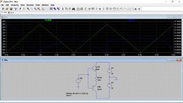
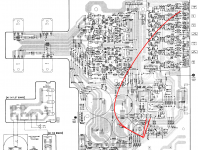
Look at this below. The base of the drivers are linked and supplied with a voltage that goes from -30 to +30 volt. The current in R519 is shown (right hand scale) and is essentially zero (femto amps) meaning zero volts across the resistor. Providing nothing is pulling current from the emitters to somewhere else then the current (and so voltage across the resistor) has to be zero.
So at this point the -0.8 volt across the resistor that you are seeing is not what I would expect.
Just out of interest is the voltage on the linked base's higher or lower than the supply to their collectors. It should not be because the circuit simply show B+ and B- as being the only rails involved but the diagram is so hard to trace that it is worth checking.
Attachments
Thanks, Just so I'm sure do you mean the leg of one of the 0.22Ohm resistor that goes to the Source of the Mosfet? ie NOT the point where the two 0.22ohm resistors are connected
It wouldn't matter for this, either leg of either resistor. The junction point is technically the best but it really wouldn't change anything here.
I do appreciate your help... But I've kind of moved onto your suggestion of removing the MOSFETS and linking the 0.22 ohm restor to the emitter of one of the driver transistors. Powers up. voltages are weird. (I've removed all MOSFETS from both channels.)
Its R521 and R621 that are 58 & 92 Ohm respectively. (not R520,R620)
Checked R521 out of cct and its 58 ohms. both Q510 & Q511 are getting hot now.
Will get back to it late tomorrow,
Its R521 and R621 that are 58 & 92 Ohm respectively. (not R520,R620)
Checked R521 out of cct and its 58 ohms. both Q510 & Q511 are getting hot now.
Will get back to it late tomorrow,
both Q510 & Q511 are getting hot now.
With the base's linked these two transistors can not 'cross conduct'. That means no current can flow in them, the only exception/s to that would be:
1/ Something is loading the emitters (so an unforeseen load). That would only heat one or other device, not both, and the level of heat would depend on the load.
Your diagram shows that with the FET's removed there is nothing there to drive.
2/ This is the weird one... if the stage was oscillating at very high frequency (100's of kHz or above) then cross conduction would occur. It is an unlikely scenario but one that is easily checked with a scope.
I'd better put link across the bases back in then, wasn't sure if mosfets removed if it was still safe to do that 🙂
OK all rebuilt. All MOSFETS removed on both channels. 0.22 ohm linked to Emittere of Q510 & Q610. Bases of Q510/Q511 and Q610/611 are connected.
"Just out of interest is the voltage on the linked base's higher or lower than the supply to their collectors. It should not be because the circuit simply show B+ and B- as being the only rails involved but the diagram is so hard to trace that it is worth checking."
Q510/511 Basea at -3.80V, Collectors are 35 and -34.8V
Q610/611 BAses at -3.97, Collectors at 34.7 & -34
Voltages across R519 is -2.76v, R619 is 3.6V
Neither LED's on the Bias cct coming on now.
Those readings seem to still show a problem around the driver stage.
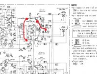
Electrically it should now look like this (attached). It doesn't matter which end of the resistors going to the driver base's you linked.
So both base's are electrically linked and so are at the same voltage. That means no current can flow in R519/619 and yet you have 2.7 and 3.6 volts.
The only 'load' being driven in this state is the feedback network and the resistive feed to the DC offset protection and both these are high value resistors drawing minimal current.
So the question is why have you got these voltages across R519/619.
If the transistors are good then we have to now suspect that the circuit is actually oscillating at some very high frequency (which would cause cross conduction in the drivers) but the only way to prove that is with a good oscilloscope of wide bandwidth to see what is there.
The theory as far as I can see is sound up to this point... no current (and hence no voltage) should be flowing in or across those resistors with the driver base's linked.
Attachments
Those readings seem to still show a problem around the driver stage.
So the question is why have you got these voltages across R519/619.
The theory as far as I can see is sound up to this point... no current (and hence no voltage) should be flowing in or across those resistors with the driver base's linked.
Could it just be the fuseable resistors being so far out of spec.
R519/R619 seem to be around 440ohms (should be 330)
R520/R521/R620 seem to be around 55ohms (should be 47)
and R621 aroun 94ohms.(should be 47)
If a fusible is out of spec then it is usually because of a previous overload, they can and do go high resistance. For fault finding you can just fit 0.25 or 0.5w standard types. They might also be going even higher resistance when power is applied.
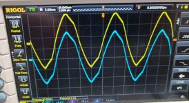
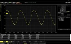
The scope seems to show just 50Hz from somewhere. What is the peak to peak amplitude on those?
5ms/div so 20ms per cycle is 50Hz. There is no sign of oscillation on that trace and 50Hz of any amplitude would not cause cross conduction, its way to slow.
I'm assuming those traces are measured from ground to each base. You can not connect a grounded scope probe (again I assume the scope is mains grounded like the amp) across a resistor because a short will be created via the scope lead and the mains lead grounds.
all fuses changed, thR621 had heat damage underneth it (It was showing 92ohms).
I'm assuming those traces are measured from ground to each base. You can not connect a grounded scope probe (again I assume the scope is mains grounded like the amp) across a resistor because a short will be created via the scope lead and the mains lead grounds
🙄, thought sony was earthed... Occiloscope on same mains, but doesn't help if sony not earthered ! duh! so was showing mains, which in itself is interesting.... hate scopes🙂
anyway how about now that probe earthered...
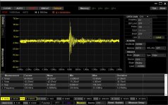
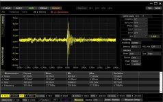
146kHz, peak to peak some 6V, between +1.3 to -4.7v
I'm assuming those traces are measured from ground to each base. You can not connect a grounded scope probe (again I assume the scope is mains grounded like the amp) across a resistor because a short will be created via the scope lead and the mains lead grounds
🙄, thought sony was earthed... Occiloscope on same mains, but doesn't help if sony not earthered ! duh! so was showing mains, which in itself is interesting.... hate scopes🙂
anyway how about now that probe earthered...
146kHz, peak to peak some 6V, between +1.3 to -4.7v
Attachments
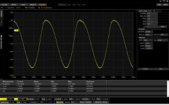
Right then... so 146kHz at the kind of amplitude you see here does show it is oscillating and that would cause the kind of effects you are seeing such as voltage over the 330 ohm.
Hmm... that is strange.
Are these two safety resistors OK? They form the Zobel network and are essential for stability. Check those first. If they are OK then we are struggling. Lets check those first though.
Hmm... that is strange.
Are these two safety resistors OK? They form the Zobel network and are essential for stability. Check those first. If they are OK then we are struggling. Lets check those first though.
Attachments
🙁 indeed. I'll have to think on this one.
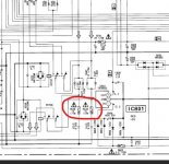
Has this amp any hidden history? has it been worked on before?
Also are both channels the same, both with the same fault in other words. If so then that would be odd.
I think you should also look with the scope at the input to the power amp just to make sure nothing is entering via that route. The connector at the top of the diagram where it is marked RV and LV. There should be no signal (that HF you measured) at those points.
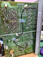
now i look at it IC801 looks like its been changed, and the black cabling on the underside looks iffy. Sounds like this may be a lost cause. BUT interesting (for me) I'll track where I think they are goin and send you a photo
in the meantime RV and LV plots....Is that just noise?
in the meantime RV and LV plots....Is that just noise?
Attachments
I assumed this was done at the factory, silly me...mainly because tape seemed to be same as that holding capacitators togeather.
I'll confirm tomorrow where it ends up at the top, hard to see.
I'll confirm tomorrow where it ends up at the top, hard to see.
Attachments
- Home
- Amplifiers
- Solid State
- Sony TA-F3000ES - doing my head in