🙁 indeed. I'll have to think on this one.
Also are both channels the same, both with the same fault in other words. If so then that would be odd.
I started from working out MOSFETS had blown, to getting it to power up without Mosfets. From memory at that point I think the voltages measured correctly on both channels. (I'm doubting that now). Put new MOSFETS back in and DBT lit up, so removed Q510/Q511, it then powered up ok, voltages on Q610/Q611 seemed ok, Q510/Q511 all over the place.
The black lead and soldering does look original and also seems to follow the white line on the PCB. I'd say that is OK.
The scope shot I'll say does look like noise but with some regular spike of something which is possibly just a measurement effect of the way it is all connected, the grounds and so on of the test set up.
IC801 is a 5v reg on the diagram, so should have a clean 5 volts coming out of it.
As to the main problem, I really don't know what to suggest tbh... well actually one more idea... instead of linking the 0.22 ohm to the emitter of the driver transistor directly lets try it via a low value resistor such as 100 ohm. Just hazy thinking that the stage might oscillate with capacitive loading on it and the resistor would isolate it from that. Beyond that... I really don't know.
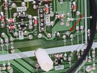
Pic 1 in post 40: between standoff and black wire, above the white line - dry joint? or is it just me? Just below R602.
if its the one with a + by the side of it, I'll check. In fact at this stage is it worth reflowing a lot of the joints?
Nr 2 to the right of the +.
I am quite lazy. Always have a good visual inspection for dry joints, hot spots, bulging caps etc before pulling out the DMM.
I am quite lazy. Always have a good visual inspection for dry joints, hot spots, bulging caps etc before pulling out the DMM.
T
As to the main problem, I really don't know what to suggest tbh... well actually one more idea... instead of linking the 0.22 ohm to the emitter of the driver transistor directly lets try it via a low value resistor such as 100 ohm. Just hazy thinking that the stage might oscillate with capacitive loading on it and the resistor would isolate it from that. Beyond that... I really don't know.
yellow is Q510. Interesting, now +-12V
R519 +4.6V, R619 +4.76V Q510->Q511, and Q610 to Q611
Attachments

Last edited:
ok I've rebuilt the "6" channel, put MOSFETS back in. Voltages seem to be about right, RED LED comes on. Without MOSFETS voltages all over the place, same as channel ".5"
Going to put CH5 MOSFETS back in. and see what happens.
IF the DBT lights up, I think all I need to do is lift one of the sides of R510 and R511, that should stop the MOSFETS from conducting?
Going to put CH5 MOSFETS back in. and see what happens.
IF the DBT lights up, I think all I need to do is lift one of the sides of R510 and R511, that should stop the MOSFETS from conducting?
R510 and 511. R510 sets a current source value and R511 would remove the supply from the front end differential stage.
In all honesty this is one that isn't looking to hopeful to diagnosing at the end of a keyboard 🙁
In all honesty this is one that isn't looking to hopeful to diagnosing at the end of a keyboard 🙁
I should have said that removing those resistors isn't a good imo. The only safe way to stop the output FET's conducting is to tie the gate and source together... but in circuit that would load the driver stage.
Red arrow indeed, and not at all. I am seated far from my screen and may be wrong😉your eyes are better than mine 😀
Is it the one pointed to by red arrow?
yep, its fine, its the angle of the photo. Anyway whats left aprt from checking the transistors, hay ho Q504 isn't right.
Using Diuode check on multimeter
BtoC 0.68V, BtoE 1.29V
CtoE 0.68V, CtoB OC as are EtoC and EtoB
When Removed Peak DCA75 says its a double diode
Q604 seems to test ok, I haven;t removed it.
BtoC 0.66V, BtoE 0.66V
CtoE OC, CtoB OC
EtoC and EtoB about 1.2V
I suppose I'd better check the others, unless any bright spark, says yes that would do it....😀
Q504 looks to be used as another current source. Base is fixed by the Zener and the current is effectively the Zener voltage less 0.6V divided by R507.
It is a critical part... and I wonder why they call everything 'protect'.
It is a critical part... and I wonder why they call everything 'protect'.
Well, I can't read that actually was a D504
 , so red herring. So, putting glasses back on I went hunting once more.
Hurrah, or not really. D505 is around the wrong way!
It’s a SEL1501C. Lesson to be learned here, what's been changed if anything. I ASSUMED that the red and green LEDS D505 and D605 were different colours to help distinguish between the channels, silly me. Both are SEL1501C.I think they are non-tinted green with a Vf of 2v.
Red tinted one (D605) was 1.96v and around the right way, clear one was suspect at 7.6V!. Anyway I' replaced both with a Square green LED at 1.96V Vf. and lo and behold both channel voltages behave the same without MOSFETS.
Short Emitter of Q510 & Q610 to Bias connector between both 0.22ohm resistors. Both channels behave roughly the same. Put MOSFETS back into "6" channel and voltages back to where they should be!.
Mostfets back into channel "5". It doesn't light up the DBT . Q512/Q513 get rather hot compared to Q612/Q613.
onwards and upwards.
No1 lesson: identify what’s been changed, don't assume anything..... (D605 looked like it had been changed, D505 didn't but must have been....)
Attachments
Last edited:
Well done finding that reverse diode 
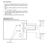
The forward voltage will determine the current in that chain and so to the bias voltage developed... so first check is to see if the bias current preset adjusts correctly by monitoring the voltage across the appropriate 0.22 ohm. The manual should say what the correct figure is.
The forward voltage will determine the current in that chain and so to the bias voltage developed... so first check is to see if the bias current preset adjusts correctly by monitoring the voltage across the appropriate 0.22 ohm. The manual should say what the correct figure is.
Of course the truth is I'm almost at the start with this amplifier. Turned both Bias trimmers to minimum. I was under the impression that once the Bias was set it was steady.
Channel "6" nothing for a while, and once you turn it around so above 15mV it comes to a point that it just keeps going.
Channel "5" never goes above 4mV.
So question is should it be a steady 20mV, or aim for 20mV within 5 seconds and doesn't matter that it keeps going.
Also the 0.22ohm resistors seem to be more like 0.33 ohms...
Attachments
Firstly you might find that an inability for the bias trimmer to reach the value needed could be down to different replacement semiconductor tolerances. Things like that current sink (the LED) will have a big impact if the current in that chain is even a little different.
Also different devices and transistor types can have slightly different turn on voltages.
As to the current not being stable... well that comes down to the design and how the bias generator senses temperature. It might keep going up for a while and then as the heat stabilises the current levels off and starts to fall again I'm afraid its an unknown (to me) what would be normal for it.
If any channels are original in all respects then use those as a guide to see what happens.
What you must ensure is that thermal runaway does not occur and that the current is reasonable even the amp is really hot.
"So question is should it be a steady 20mV, or aim for 20mV within 5 seconds and doesn't matter that it keeps going"
So is the bias voltage rising a sign of thermal runaway?
We are measuring voltage across a 0.22ohm resistor, so 20mV would give 0.1A. That doesn't seem large to me... was going up quite quickly tho
So is the bias voltage rising a sign of thermal runaway?
We are measuring voltage across a 0.22ohm resistor, so 20mV would give 0.1A. That doesn't seem large to me... was going up quite quickly tho
Last edited:
Thermal runaway generally means it keeps increasing continually to damaging levels.
Poor thermal design means it increases until thermal equilibrium is reached. It may rise initially as the output devices heat and then start to fall back as the bias generator also warms and reduces the bias voltage. In most amps TR5/614 would be in contact with the heatsink to sense the temperature.
You will have to just see what happens. If it gets to 40mv then that is nearly 200 milliamps flowing... which is not that high in the scheme of things but high enough to heat things up. It is about 8 watts per output transistor.
If it gets that high and then falls back then that is fine. If it keeps going then that isn't good.
- Home
- Amplifiers
- Solid State
- Sony TA-F3000ES - doing my head in