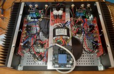
I would like to share this my new project because it sound very good and it is cheap and simple.
After the good experience made on hybrid amplifiers with circlotron configuration I thought about making a completely solid state amplifier of this type.
It is the result of many months of simulations, instrumental testing and listening test.
This is not a common solid state amplifier with lot of global feedback, there are only 6dB to reduce output impedance and to linearize the voltage stage.
You can increase the output power to 60W on 8ohm changing the chassie and increasing the power supply voltage of the output stage.
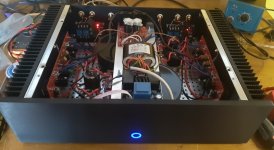
I have used the chassie HiFi 2000
Dissipante 03/300B 3U 10mm BLACK
Product Code: 1NPD03300B or 1NPD03300N
Inner baseplate for Dissipante 300mm
Product Code: 1BASEPD300
Specifications:
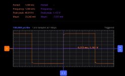
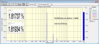
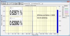
Pout = 50W on 8ohm with 2 x 33VDC and Vin=0.42Vrms Thd=0.6%
Pout = 90W on 4ohm with 2 x 33VDC and Vin=0.42Vrms Thd=1.3%
Pout = 18W on 8ohm no-switching with 1A bias (see simulation)
Pd = output stage at 35VDC = 70W each channel with 1A bias
Zout = 178mohm with the Exicon (see simulation)
Ft(-3dB) = DC - 2MHz at -3dB
Global feedback = 6dB
Output DC offset about 50-90mVDC (because there is no active DC servo)
These are the main characteristics:
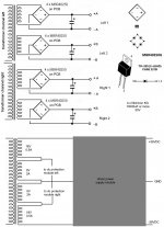
These are the components used for the pcb.
J1,J2,J3 J113D74Z
T1,T2 BC546ABU
T3,T4,T5,T6 BC556B
T7,T8 MJE340
U$1,U$2 ECW20N20-S or ECW20N20 or 2SK1058
R1,R2 100Kohm 1% 1/4W Vishay Dale RN55
R3,R4,R7 1Kohm 1% 1/4W Vishay Dale RN55
R8 500ohm 1% 1/4W Vishay Dale RN55
R5,R6 47ohm 1% 1/4W Vishay Dale RN55
R13,R14 470ohm 1% 1/4W Vishay Dale RN55
R9,R10,R11,R12 15Kohm 1% 1/4W Vishay Dale RN55
R17,R18 3900ohm 1% 1/4W Vishay Dale RN55
R15,R16 10Kohm 1% 1/2W Vishay Dale RN65
R19,R20 2700ohm 5% 2W Vishay PR02
R21,R22 2000ohm 1% 1/4W Vishay Dale RN55
R23,R24 120 or 240ohm 1% 1/4W RN55 bias 120ohm with ECW20N20
R28,R29 900ohm 1% 1/4W Vishay Dale RN55
R25,R31 1Kohm multi turn trimmer Bourns 3296W-1-501LF
RGND 100ohm 1% 1/4W Vishay Dale RN60 (not necessary for dual mono conf.)
RGROUND 10ohm 5% 2W Vishay PR02 (see photo)
C1,C2 100uF 50V UFG Nichicon
C3,C4 1uF MKP or MKT
C5,C6 not used
CIN 1uF MKP or MKT to use in parallel to R2 if only un-bal input is used
F1,F3 FUSE 5A FAST
KK1,KK4 HEATSINK SK104 13.4C/W 513002B02500G (cod. MOuser 532-513002B25G)
The connections are 63862-1 (CUT STRIP) by TE Connectivity / AMP (cod. Mouser 571-63862-1-CT, cod. RS 718-7987)
CZ 0.1uF Vishay F339X1
RZ 10ohm 2W Vishay PR02
Available the LTspice files and all the measurements with ECW20N20 and 2sk1058 .
After the good experience made on hybrid amplifiers with circlotron configuration I thought about making a completely solid state amplifier of this type.
It is the result of many months of simulations, instrumental testing and listening test.
This is not a common solid state amplifier with lot of global feedback, there are only 6dB to reduce output impedance and to linearize the voltage stage.
You can increase the output power to 60W on 8ohm changing the chassie and increasing the power supply voltage of the output stage.
I have used the chassie HiFi 2000
Dissipante 03/300B 3U 10mm BLACK
Product Code: 1NPD03300B or 1NPD03300N
Inner baseplate for Dissipante 300mm
Product Code: 1BASEPD300
Specifications:
Pout = 50W on 8ohm with 2 x 33VDC and Vin=0.42Vrms Thd=0.6%
Pout = 90W on 4ohm with 2 x 33VDC and Vin=0.42Vrms Thd=1.3%
Pout = 18W on 8ohm no-switching with 1A bias (see simulation)
Pd = output stage at 35VDC = 70W each channel with 1A bias
Zout = 178mohm with the Exicon (see simulation)
Ft(-3dB) = DC - 2MHz at -3dB
Global feedback = 6dB
Output DC offset about 50-90mVDC (because there is no active DC servo)
These are the main characteristics:
- dc coupled of all stages
- no capacitors on the signal path
- high slew-rate
- good damping factor near to a solid state amplifiers with high feedback
- no switching output stage like a pure class A
- high efficiency because only 70W of consumption per channel
- only single ended stages
- only a single output device
- only a transconductance amplifier with I/V
- global feedback easy to modify without high frequency compensation
- full balanced circuit but it accept also un-balanced input signal
These are the components used for the pcb.
J1,J2,J3 J113D74Z
T1,T2 BC546ABU
T3,T4,T5,T6 BC556B
T7,T8 MJE340
U$1,U$2 ECW20N20-S or ECW20N20 or 2SK1058
R1,R2 100Kohm 1% 1/4W Vishay Dale RN55
R3,R4,R7 1Kohm 1% 1/4W Vishay Dale RN55
R8 500ohm 1% 1/4W Vishay Dale RN55
R5,R6 47ohm 1% 1/4W Vishay Dale RN55
R13,R14 470ohm 1% 1/4W Vishay Dale RN55
R9,R10,R11,R12 15Kohm 1% 1/4W Vishay Dale RN55
R17,R18 3900ohm 1% 1/4W Vishay Dale RN55
R15,R16 10Kohm 1% 1/2W Vishay Dale RN65
R19,R20 2700ohm 5% 2W Vishay PR02
R21,R22 2000ohm 1% 1/4W Vishay Dale RN55
R23,R24 120 or 240ohm 1% 1/4W RN55 bias 120ohm with ECW20N20
R28,R29 900ohm 1% 1/4W Vishay Dale RN55
R25,R31 1Kohm multi turn trimmer Bourns 3296W-1-501LF
RGND 100ohm 1% 1/4W Vishay Dale RN60 (not necessary for dual mono conf.)
RGROUND 10ohm 5% 2W Vishay PR02 (see photo)
C1,C2 100uF 50V UFG Nichicon
C3,C4 1uF MKP or MKT
C5,C6 not used
CIN 1uF MKP or MKT to use in parallel to R2 if only un-bal input is used
F1,F3 FUSE 5A FAST
KK1,KK4 HEATSINK SK104 13.4C/W 513002B02500G (cod. MOuser 532-513002B25G)
The connections are 63862-1 (CUT STRIP) by TE Connectivity / AMP (cod. Mouser 571-63862-1-CT, cod. RS 718-7987)
CZ 0.1uF Vishay F339X1
RZ 10ohm 2W Vishay PR02
Available the LTspice files and all the measurements with ECW20N20 and 2sk1058 .
Attachments
-
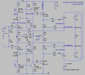 SolidState2022_sch.jpg92.9 KB · Views: 3,839
 -
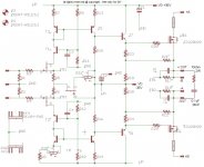 SolidState2022_ver13_sch.jpg89 KB · Views: 3,947
 -
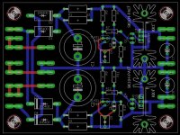
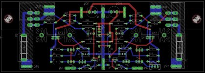 SolidState2022_ver13_pcb.jpg178.9 KB · Views: 2,965
 -
 SolidState2022a_thd_8ohm_20Vrms.jpg92.3 KB · Views: 1,950
 -
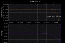 SolidState2022a_freq_8ohm.jpg64 KB · Views: 1,606
 -
 SolidState2022_square_8ohm_Exicon.jpg61.7 KB · Views: 3,219

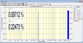
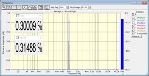
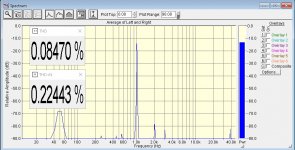
Hmmm….. 50W/8ohm/1kHz THD of 0.6% ….. this is not good. Even if we lived in 1965. And why your spectrum is cut at -55dBr, some nasty spectral lines below?
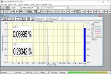
1W and 50W thd on 8ohm
I can share the pcb files
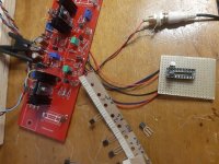
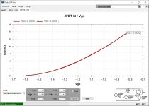
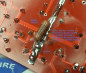
The J113 must be selected with a manual test or with an instrument to get the best result
I can share the pcb files
The J113 must be selected with a manual test or with an instrument to get the best result
Attachments


The driver stage need a regulated power supply module to have a stable +36VDC and -36VDC.
The normal linear regulator does not support 40V input so I have design a shunt regulator following the application note in the datasheet of TL431 and I have optimized this circuit with LTspice.
D1,D2,D3,D4 UF5407
C1,C2 4700uF 50V +105°C Nichicon 20 x 40mm
C3,C6 10pF
C4,C5 1nF
R1,R2,R3,R4 47ohm 1W (use only R1 and R4 for dual mono configuration)
U$1,U$2 TL431
R5,R9 1Kohm 1% 1/4W
R8,R11 15Kohm 1% 1/4W
R6,R10 1100ohm 1% 1/4W
R7,R12 100ohm 1% 1/4W
Q1,Q4 BC556
Q2,Q3 MJE350
C7,C8 22uF 50V UFG Nichicon
KK1,KK4 HEATSINK SK104 11C/W 513102B02500G (cod. MOuser 532-513102B25)
Attachments

Foer the power transformers the my choice is a pair of RS Pro Encapsulated Transformers 2 x 25V 225VA (cod. RS RS123-4028)
The transformer for the driver stage is the LITE R26-10 (diyclub.biz) an r-core 30VA with 2 x 9V 3A and 2 x 18V 0.5A
The transformer for the driver stage is the LITE R26-10 (diyclub.biz) an r-core 30VA with 2 x 9V 3A and 2 x 18V 0.5A
Attachments
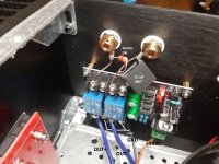
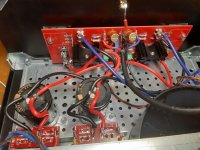
STARTUP PROCEDURE
1. Verify the power supply voltage on driver power module +36VDC and -36VDC
2. Set both trimmers in the middle, both the end of the path can be identified by listening to the slight click
3. Connect a multimeter at the connection point between R23 - R28 and ground
4. Give the power supply only to the driver stage
5. Rotate the R31 trimmer until you read a voltage near the 0v
6. Connect a multimeter at the connection point between R29 - R24 and ground
7. Rotate the R25 trimmer until you read a voltage near the 0v
8. Repeat again point 5 and 7 until you read about 0v on both these points
9. add a 0.1ohm in series to the mosfet power supply so on the connection before one fuse to very the bias current of output
10. Connect the power supply to the output stage
11. Turn the trimmer R31 to read 0V on terminal OUT1
12. Turn the trimmer R25 to read 0V on terminals OUT1 and OUT2
13. Check again both these points and modify the trimmer position if necessary
14. Verify the bias current measuring the voltage across the 0.1ohm resistance
Do you have a link?pcb are available on ebay shop
I don't get money from this shop
Interesting design, Andrea, and quite low distortion with no fb applied. I like the low parts count, lack of source resistors on the outputs, high linearity, speed, non-switching, and relative simplicity. I would prefer H2 dominant rather than H3, and like to see the harmonics down to -130dB on the range (PMA's comment), but I would expect it to sound very good despite highish THD.....
I have been aware of your website and designs for decades and always liked your power buffer, not to mention your concept of sliding bias on drivers with diamond buffers, which works very well.
Salute to an unconventional design, your creativity, and your generosity publishing it on this forum. This approach reminds me of an amp from Valery, who sadly died a year ago in Moscow.
Ciao,
HD
Yes, but the OLG of this amp is little more than CLG so it's defined as very low fb.
It is a very good circuit in my opinion.
HD
It is a very good circuit in my opinion.
HD
I fully agree with you about H2 dominant but just don't select the fet to get the desired effect and this give a less neutral but more pleasant to listen especially with normal digital sources.Interesting design, Andrea, and quite low distortion with no fb applied. I like the low parts count, lack of source resistors on the outputs, high linearity, speed, non-switching, and relative simplicity. I would prefer H2 dominant rather than H3, and like to see the harmonics down to -130dB on the range (PMA's comment), but I would expect it to sound very good despite highish THD.....
I have been aware of your website and designs for decades and always liked your power buffer, not to mention your concept of sliding bias on drivers with diamond buffers, which works very well.
Salute to an unconventional design, your creativity, and your generosity publishing it on this forum. This approach reminds me of an amp from Valery, who sadly died a year ago in Moscow.
Ciao,
HD
Here follows the plot in these 2 conditions no matched fet and matched fet, the thd value was measured near the power supply limit.
Attachments
- Home
- Amplifiers
- Solid State
- Solidstate 2022 - Hi-end amplifier