Yes PS - A wilson CM is better than that enhanced widlar.OS
Complementary diff pair inputs create additional CM design challenges.
The 3-transistor Wilson current mirror has a 2Vbe drop on just one side, and this has affected my efforts to get a safe start-up with complementary diff pair inputs.
The 4-transistor "improved" Wilson current mirror has a balanced 2Vbe drop on each side. In my designs, this 2Vbe drop increases distortion due to reduced VAS stage drive voltage.
Does anyone have a clever complementary diff pair input design using improved 4-transistor Wilson current mirrors?
I never used the 4Q-CM , but the blameless shows the same 6ppm THD20
with or without it.
It clips more assymetrically w/ the 2 vbe drop and you need 1 diode ..
but all else remains the same. You will get less of a voltage swing ..
THD stays the same right up until you hit that 2 vbe "penalty". Same
as a cascoded VAS ... I get a 3.1V "penalty" - I just use a higher V supply.😀
OS
Attachments

Complete amp....
Believe me , I did not do this for the forum !
I now have enough to share - If they care (and not "lurk").
Here , and only here .. can you build an amp and not take a leap of
faith.
If you don't like "X" CFA or VFA ..."yank it", mine it for parts , and build the
next one. The fine EF3 (triple), only magnifies >25K whatever the bloody
VAS sends to it.
It will fit standard 250mm 3-5H heatsinks or with 90 degree IPS setup ,
a 200mm long heatsink. Same as my "supersym" years ago (where the
"badger" came from) , but 3 years more advanced.
I'll share some of my IPS's (over 30 now). Most are 10-16 device ,
3 CFA (now) and 25+ VFA.
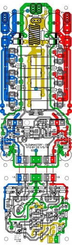
Also have 5 pair "slewmaster" OPS layout.
Just a little more "housekeeping" 🙂 .
OS
Believe me , I did not do this for the forum !
I now have enough to share - If they care (and not "lurk").
Here , and only here .. can you build an amp and not take a leap of
faith.
If you don't like "X" CFA or VFA ..."yank it", mine it for parts , and build the
next one. The fine EF3 (triple), only magnifies >25K whatever the bloody
VAS sends to it.
It will fit standard 250mm 3-5H heatsinks or with 90 degree IPS setup ,
a 200mm long heatsink. Same as my "supersym" years ago (where the
"badger" came from) , but 3 years more advanced.
I'll share some of my IPS's (over 30 now). Most are 10-16 device ,
3 CFA (now) and 25+ VFA.
Also have 5 pair "slewmaster" OPS layout.
Just a little more "housekeeping" 🙂 .
OS
Attachments
Last edited:
Complete amp....
Believe me , I did not do this for the forum !
I now have enough to share - If they care (and not "lurk").
Here , and only here .. can you build an amp and not take a leap of
faith.
If you don't like "X" CFA or VFA ..."yank it", mine it for parts , and build the
next one. The fine EF3 (triple), only magnifies >25K whatever the bloody
VAS sends to it.
It will fit standard 250mm 3-5H heatsinks or with 90 degree IPS setup ,
a 200mm long heatsink. Same as my "supersym" years ago (where the
"badger" came from) , but 3 years more advanced.
I'll share some of my IPS's (over 30 now). Most are 10-16 device ,
3 CFA (now) and 25+ VFA.
Also have 5 pair "slewmaster" OPS layout.
Just a little more "housekeeping" 🙂 .
OS
I think that your feedback path is to long, I would put up side down the part with the output transistors so that inductor is close to the drivers.
BR Damir
can I buy the cfa pcb from you? IPS and OPS?
Thx-RNMarsh
If you have a printer , you can print one.
Let me get the "top gun" VFA out there (most likely a blameless/badger Varient).
I will zip the hi-rez PCB-BOM-schema of the "slewmaster" OPS first.
Then the IPS's - same deal.
If the store would want it , I would , AJT.By AJT -are you making this design available at the diyaudio store?
I think these modular creations have all the advantages of a complete board
with none of the disadvantages. The ND-/PD+ run 50mm along side of 0V and
regulated rails. NO noise or corruption here - IPS also has local decoupling
and further regulation.
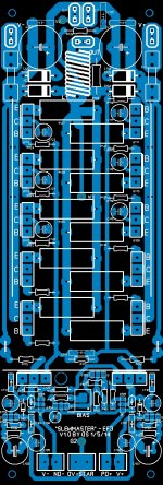
Here's the 5 pair OPS -
OS
Attachments
I think that your feedback path is to long, I would put up side down the part with the output transistors so that inductor is close to the drivers.
BR Damir
Thanks for the comment... "I think? " It (the NFB path) is center point and
"floating" 30mm off the OPS PCB at very low-Z.
The NFB path will "float" back to the IPS and have the first FB divider R
30mm away from the IPS PCB.
Would you have an amp output wire lie directly across your input section ?
"Mutual induction"... One "player" is the coil - the other is the trace.
This might be the same effect as having the OP inductor anywhere within
30mm or so of ANY hi-Z section (vbe - predrivers). EF2 is MUCH less prone to
this issue.
On a full board , I would reduce the NFB to 1-2V (like J.Didden proposed) before routing back to the IPS.
Imagine having the (real dirty EM) Inductor at 10A peak next to the triple's Vbe.
30nA drive current is easily "disturbed" (below) ! 😱
EVERY OEM has the inductor as far from the IPS as possible , most don't
even have it near the OPS .... usually back near the speaker terminals/unregulated power supply.
Some even put it on a separate PCB.
On the "badger" PCB ,both the IPS/VAS and EF driver traces are at least 25mm
away from the Inductor. The only trace that comes near is the NFB ... which
then jumps a ground with the first FB divider resistor -ideal !
Halcro runs the OP (shielded) to another "chamber"
,EM shields that chamber ... and puts the inductor in there. 😀
OS
Attachments
If you have a printer , you can print one.
OS
?? Print one ?? and actually go out and buy acid, copper, drills and bits, etc?? Who? Me?? I don't think so.
But, if you make a set for your self, make an extra one for me and I'll buy it from you. I want to measure all the designs shown here... esp CFA.
Thx-RNMarsh
?? Print one ?? and actually go out and buy acid, copper, drills and bits, etc?? Who? Me?? I don't think so.
But, if you make a set for your self, make an extra one for me and I'll buy it from you. I want to measure all the designs shown here... esp CFA.
Thx-RNMarsh
We could easily have a few made in China using a resource that I regularly use. That wouldn't cost much. They'd charge a standard setup fee ($75 or so) and a few dollars per board for each one they make.
The 5 pair OPS looks interesting to me. I am looking forward to studying the details of that once OStripper posts the details
We could easily have a few made in China using a resource that I regularly use. That wouldn't cost much. They'd charge a standard setup fee ($75 or so) and a few dollars per board for each one they make.
🙂
Now That's a plan I can go for.
Thanks - Richard
Thanks for the comment... "I think? " It (the NFB path) is center point and
"floating" 30mm off the OPS PCB at very low-Z.
The NFB path will "float" back to the IPS and have the first FB divider R
30mm away from the IPS PCB.
Would you have an amp output wire lie directly across your input section ?
"Mutual induction"... One "player" is the coil - the other is the trace.
This might be the same effect as having the OP inductor anywhere within
30mm or so of ANY hi-Z section (vbe - predrivers). EF2 is MUCH less prone to
this issue.
On a full board , I would reduce the NFB to 1-2V (like J.Didden proposed) before routing back to the IPS.
Imagine having the (real dirty EM) Inductor at 10A peak next to the triple's Vbe.
30nA drive current is easily "disturbed" (below) ! 😱
EVERY OEM has the inductor as far from the IPS as possible , most don't
even have it near the OPS .... usually back near the speaker terminals/unregulated power supply.
Some even put it on a separate PCB.
On the "badger" PCB ,both the IPS/VAS and EF driver traces are at least 25mm
away from the Inductor. The only trace that comes near is the NFB ... which
then jumps a ground with the first FB divider resistor -ideal !
Halcro runs the OP (shielded) to another "chamber"
,EM shields that chamber ... and puts the inductor in there. 😀
OS
OK, I don't talk about inductor(inductor was just indication of position) but the feedback long track, you can put inductor outside the amp board.
Thanks for the comment... "I think? " It (the NFB path) is center point and
"floating" 30mm off the OPS PCB at very low-Z.
The NFB path will "float" back to the IPS and have the first FB divider R
30mm away from the IPS PCB................
OS
I think Dadod was referring to the spatial dimension of the loop that the sample current over the NFB divider has to go around. CFAs usually have at least an order of magnitude lower value resistors in the NFB divider than would a VFA, the sample current is therefore at least 10x as well. On top of that, we are also dealing with, say, 3x as much V/uS transitions at the output as usually do a VFA. These 10x greater current and several 10x greater di/dt perhaps begin to make the efforts worthwhile in keeping a minimized loop area (impedance) of the current loop and not sharing the ground return path with the front end.
By the way, the DC blocking capacitor C3 in the NFB divider is subject to the big NFB sample current and much elevated di/dt. Is it possible to get rid of such a potential performance bottleneck and instead make the amp DC-coupled?
Your neat, simplicity style of layout and modular construction is quite impressive.
I agree,you can put inductor outside the amp board.
Put inductor in the protection/switching pcb/section of the design.
Keep FB node as short as possible. Could refer to the Mark Alexsander CFA PA layout from long ago. Looks to be less than 2" long.
Care to share your source?We could easily have a few made in China using a resource that I regularly use.
We could easily have a few made in China using a resource that I regularly use. That wouldn't cost much. They'd charge a standard setup fee ($75 or so) and a few dollars per board for each one they make.
The 5 pair OPS looks interesting to me. I am looking forward to studying the details of that once OStripper posts the details
Perhaps if OS would make the Gerber and Excellon files available when all is 100% QC'd then those who are willing to send out for boards could do so...
I think Dadod was referring to the spatial dimension of the loop that the sample current over the NFB divider has to go around. CFAs usually have at least an order of magnitude lower value resistors in the NFB divider than would a VFA, the sample current is therefore at least 10x as well. On top of that, we are also dealing with, say, 3x as much V/uS transitions at the output as usually do a VFA. These 10x greater current and several 10x greater di/dt perhaps begin to make the efforts worthwhile in keeping a minimized loop area (impedance) of the current loop and not sharing the ground return path with the front end.
By the way, the DC blocking capacitor C3 in the NFB divider is subject to the big NFB sample current and much elevated di/dt. Is it possible to get rid of such a potential performance bottleneck and instead make the amp DC-coupled?
Your neat, simplicity style of layout and modular construction is quite impressive.
Thanks for comment. Actually , The shorter NFB is "cooler" (layout wise")
I agree !! Would 70mm be short enough ? I changed the layout without
a major overhaul. (look below)
As a compromise , the OP/center point trace to the inductor is now the "long one". As
it is allowed (even preferred) to place the above inductor in a far away place,
all is cool ?
C3 can be omitted , the simulation runs the same without it after setting
the offset trimmer. Better to be safe than sorry.
With C3 .clipping is more symmetrical - the reason I included it.
OS
Attachments
If you have a printer , you can print one.
Let me get the "top gun" VFA out there (most likely a blameless/badger Varient).
I will zip the hi-rez PCB-BOM-schema of the "slewmaster" OPS first.
Then the IPS's - same deal.
If the store would want it , I would , AJT.
I think these modular creations have all the advantages of a complete board
with none of the disadvantages. The ND-/PD+ run 50mm along side of 0V and
regulated rails. NO noise or corruption here - IPS also has local decoupling
and further regulation.
Here's the 5 pair OPS -
OS
are you giving away pdf files of board lay-out?
i would like to try making one using the toner transfer method,
i have some FR4 blanks to use...
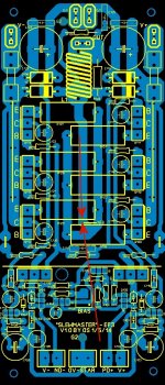
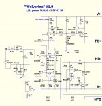
Enter "the WOLVERINE"
Just a little nastier than cousin Badger ....Enter - the "Wolverine". 😀
All "flipped" around , we can now listen to the goodness of the KSC3503 for
VAS and many common PNP's for LTP.
The Wolverine is a tougher breed , clip it all day with it's active saturation
clamp. Dadod's buffered LED cascode will light the way to audio ecstasy.
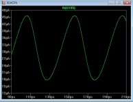
(Below 1) is schema .... 14 semi's/27 resistors/10 caps/6 diodes (4 led's)
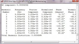
A nice 4 ppm 3R THD20 1/2 throttle. (below 2-with EF3)
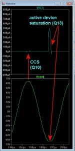
(below 3) is the "clamping action" ... it is so quick it even clamps a little on
the minor saturation of the CCS (Q9/10) , C10/R23 dampen the action a little
to minimize any artifacts. With no clipping ... C10,R23,R22, and Q11 are "not there" , showing only pA's of current.
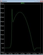
(Below 4) is symmetrical +62.7V/-63V clamped clip behavior. Slightly more
aggressive than the badger - Slew is healthy 100V+/us.... UG is 815Khz.
Sehr Gut. In every way. Any ideas welcome (simple ones 😱 ) 😀
Edit - R27 plot/attachment 3 is actually R23 on schema.
OS
Just a little nastier than cousin Badger ....Enter - the "Wolverine". 😀
All "flipped" around , we can now listen to the goodness of the KSC3503 for
VAS and many common PNP's for LTP.
The Wolverine is a tougher breed , clip it all day with it's active saturation
clamp. Dadod's buffered LED cascode will light the way to audio ecstasy.
(Below 1) is schema .... 14 semi's/27 resistors/10 caps/6 diodes (4 led's)
A nice 4 ppm 3R THD20 1/2 throttle. (below 2-with EF3)
(below 3) is the "clamping action" ... it is so quick it even clamps a little on
the minor saturation of the CCS (Q9/10) , C10/R23 dampen the action a little
to minimize any artifacts. With no clipping ... C10,R23,R22, and Q11 are "not there" , showing only pA's of current.
(Below 4) is symmetrical +62.7V/-63V clamped clip behavior. Slightly more
aggressive than the badger - Slew is healthy 100V+/us.... UG is 815Khz.
Sehr Gut. In every way. Any ideas welcome (simple ones 😱 ) 😀
Edit - R27 plot/attachment 3 is actually R23 on schema.
OS
Attachments
Last edited:
are you giving away pdf files of board lay-out?
i would like to try making one using the toner transfer method,
i have some FR4 blanks to use...
You might like the above posted circuit - the next gen. badger 🙂 .
Wait till I get a little more feedback from local "guru's" - finalize/package/
triple check.
If you read the main badger sticky ... you will see the process. When it was finally submitted (badger) ... worked the first time - no issues.
I will post what I promised on the thread title ... a VFA , a CFA , and a bad ar$e
output stage that will run them both !! 😀
OS
- Home
- Amplifiers
- Solid State
- Slewmaster - CFA vs. VFA "Rumble"