Cool Terry , you have yours going .. too !!
I try real hard to have first time successes for these designs. I was a little
worried.
I'm doing the second "kypton" now. I now know the VAS is real good ..
V will have the same design.
I redesigned the VAS (layout wise) , transistor/heatsink issue is solved.
I will use the same for all kyptons (below).
PS - I have the "C" redesigned fully for toner DIY - all errata corrected.
(below Attached)
OS
Attachments
Now it is confirmed that my suggestion to use Baxandall super pair VAS to get good clipping is not only simulation artifact, thank you thimios and to OS too.
Damir
You were right on the money ! PS - I read your threads carefully , many good ideas 😉 !
OS
Hey Pete, That looks better. I mounted the the heatsink to the top them and it gets warm so I think it is probably a good idea for longevity. A whole lot less confusing this way too. Glad I could be a part.
For the NFB I have 2k2/68R in there. Do you think that is OK?
Thanks, Terry
For the NFB I have 2k2/68R in there. Do you think that is OK?
Thanks, Terry
ostripper
Sory for small offtpic. I would be very happy If You will can help me a bit.
I am trying to do my first hybrid and i do not know how to ged rid of the crossover distortions spikes (I am not sure about it) in the input stage. There seems to be nothing bad happening in output stage but two front LTP currents arent looking good.
*.asc file is in zip.
Big thanks.
Peter
You had a .inc file in the zip.
But I know of these things.
Some my high gain IPS's will do this at high power levels. Your example
is extreme.
I see you are using lead compensation to "tame" the 2 stage LTP. You
are feeding the higher order X-over "garbage" right back to your first
LTP - It is responding accordingly.
These 2 stage LTP's are quite sensitive (and harder to compensate).
Try a local compensation FB loop instead. (2-10pF from VAS to inverting
input).
OS
Hey Pete, That looks better. I mounted the the heatsink to the top them and it gets warm so I think it is probably a good idea for longevity. A whole lot less confusing this way too. Glad I could be a part.
For the NFB I have 2k2/68R in there. Do you think that is OK?
Thanks, Terry
2.2K/82R is 27X gain 2.2K/68R is 30+X gain , either is OK.
On this amp , going for 1K/39R or 1.5K/56R will increase slew mostly.
The baxandall (super-pair) does not need all that "current on demand".
It's beta enhanced , needing only uA drive current.
If any try (1K/39R or 1.5K/56R) , R7/9 needs to be 8.2K and C13/14 =
39-47pF to retain stability.
2.2K/82R seems to be the best compromise between cool resistors ,
margin , gain , and slew.
OS
You had a .inc file in the zip.
But I know of these things.
Some my high gain IPS's will do this at high power levels. Your example
is extreme.
I see you are using lead compensation to "tame" the 2 stage LTP. You
are feeding the higher order X-over "garbage" right back to your first
LTP - It is responding accordingly.
These 2 stage LTP's are quite sensitive (and harder to compensate).
Try a local compensation FB loop instead. (2-10pF from VAS to inverting
input).
OS
Just my 2 cents, if I may... 😉
In addition to what OS just mentioned, there is one more point for improvement. Your tube LTP has got a slightly positive bias (grid voltage is more positive than the cathode one). It't better to have the tube negatively biased (around +1V at the cathodes) - this will ensure a better working point and prevent from the grid currents. Also, minimal anode voltage (for maintaining linearity) for 12AU7 is around 28V. Slight reduction of the tale current will solve both issues (R7 increase). Hope this helps 😎
Borys was not "off topic" . The tube front end is like the JFET input pair.
This is what the Japanese used in most of these designs , anyways .
(not the tubes - except for in 1 70's luxman 😱)
I am so impressed with the performance with ANY of my FET models ,
the "Kypton-V" will have a optional Jfet 1st stage (below).
The JFET simulations have 2 effects.
-They do increase distortion slightly ... 9ppm to 16ppm 20K (so what).
-H2 rises , the "tube sound" 😕 ?
-degenerate sources (less -22R) and increase Id to 2ma
All else is real good - offset , clip , slew.
OS
Attachments
Borys was not "off topic" . The tube front end is like the JFET input pair.
This is what the Japanese used in most of these designs , anyways .
(not the tubes - except for in 1 70's luxman 😱)
I am so impressed with the performance with ANY of my FET models ,
the "Kypton-V" will have a optional Jfet 1st stage (below).
The JFET simulations have 2 effects.
-They do increase distortion slightly ... 9ppm to 16ppm 20K (so what).
-H2 rises , the "tube sound" 😕 ?
-degenerate sources (less -22R) and increase Id to 2ma
All else is real good - offset , clip , slew.
OS
Is there a Jfet that is available that will work? That one is listed as obsolete everywhere.
Is there a Jfet that is available that will work? That one is listed as obsolete everywhere.
Nearly any I have tried work well.
I'm making the board for cheap , easy to source fairchild J111-113.
The first stage uses a 15V supply - any of mousers 105 n-channel fet's.
the FET only sees 7 volts Vds in the circuit - perfect.
ON semi has the 2sk596 http://www.mouser.com/ds/2/308/ENA0944-D-266479.pdf
Low Ciss microphone fet.
I'm sure just the OLG will be slightly affected by different Jfets (change rd).
At 7V .. electrically, all will run the amp( without smoke). No big
issue expected - BCxxx is pin for pin compatible with Jfet DGS.
OS
Everyone is scared of SMD , but they are DGS , too.
On the same pads as the to-92 , add the SOT-23 (below) ...
Then you could choose 100's more devices.
-BJT/ to-92 or SOT-23
-FET/ to-92 or SOT-23
Any device. Just change Re/Rsource to use it.
No tube - leave that to vzaichenko .... filament voltage supply BAHHH ! 🙁
OS
On the same pads as the to-92 , add the SOT-23 (below) ...
Then you could choose 100's more devices.
-BJT/ to-92 or SOT-23
-FET/ to-92 or SOT-23
Any device. Just change Re/Rsource to use it.
No tube - leave that to vzaichenko .... filament voltage supply BAHHH ! 🙁
OS
Attachments

I believe that is absolutely necessary someone draw a pcb for smd devices!Everyone is scared of SMD , but they are DGS , too.
On the same pads as the to-92 , add the SOT-23 (below) ...
Then you could choose 100's more devices.
-BJT/ to-92 or SOT-23
-FET/ to-92 or SOT-23
Any device. Just change Re/Rsource to use it.
No tube - leave that to vzaichenko .... filament voltage supply BAHHH ! 🙁
OS
OS ,Fet .....interesting!I have some 2sk146GR from an old project.
OS
Valery
THANKS for guiding me in the right dirrection.
Hope I will not blow anything up.
OS
I have tryed many different compensation types but no success (lack of my knowledge). I will make a prototype and test try to check it at the real animal.
Valery
There is online tool for the calculating the triode ''working point'' but I do not know if it is ok to use it for the input stages too. I will reduce tali current to 0.8mA per triode (than catode voltage is around 1.2V --> would it be ok ?)
http://www.trioda.com/tools/triode.html
It might be handy too.
THX
Valery
THANKS for guiding me in the right dirrection.
Hope I will not blow anything up.
OS
I have tryed many different compensation types but no success (lack of my knowledge). I will make a prototype and test try to check it at the real animal.
Valery
There is online tool for the calculating the triode ''working point'' but I do not know if it is ok to use it for the input stages too. I will reduce tali current to 0.8mA per triode (than catode voltage is around 1.2V --> would it be ok ?)
http://www.trioda.com/tools/triode.html
It might be handy too.
THX
Last edited:
OS
Valery
THANKS for guiding me in the right dirrection.
Hope I will not blow anything up.
OS
I have tryed many different compensation types but no success (lack of my knowledge). I will make a prototype and test try to check it at the real animal.
Valery
There is online tool for the calculating the triode ''working point'' but I do not know if it is ok to use it for the input stages too. I will reduce tali current to 0.8mA per triode (than catode voltage is around 1.2V --> would it be ok ?)
Triode Loadline Simulator v.2.5 (20141028 www.trioda.com)
It might be handy too.
THX
Yes, +1.2V will be fine

I believe that is absolutely necessary someone draw a pcb for smd devices!
OS ,Fet .....interesting!I have some 2sk146GR from an old project.
Thimios , oh master builder .... you are going to LOVE

 the next one.
On the Kypton-C, you can omit R28-29 ... gain will increase.
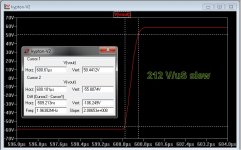
I now have 212V/uS out of a cheap japanese circuit with 100db margin.
Borys and vzaichenko , to get absolute stability out of the 2 stage LTP (below 1
example) ,tweak your main compensation (C7) with decreasing values
10p , 8.2p , 7.5p ..... until overshoot is eliminated on a full rail to rail squarewave.
I needed different values to do this with either the BJT or FET.
Once the overshoot is gone , you will still notice a small "wiggle" , even on
a nicely rounded squarewave. Adjust (increase pF) the lag (C6/R6) to
get rid of it. Also, FET was different than BJT.
What is strange , the phase margin was always excellent , even if the
transient response was less than ideal. It does not respond like a LIN
or typical CFA design ??
In the end , you will have a perfect rail to rail response with stellar slew rate.
(below 2).
I "gave up" on this type amp a few months back 😱 - now I have it.
OS
Attachments
SMD is actually easier for the home etcher. Less drilling. Buy a syringe of solder and cook it in a toaster oven. I've had great success with it.Everyone is scared of SMD , but they are DGS , too.
On the same pads as the to-92 , add the SOT-23 (below) ...
Then you could choose 100's more devices.
-BJT/ to-92 or SOT-23
-FET/ to-92 or SOT-23
Any device. Just change Re/Rsource to use it.
No tube - leave that to vzaichenko .... filament voltage supply BAHHH ! 🙁
OS
OS ,finally these resistors R29,29 (680K)must be populated or not?
I'll have to try pulling those in the morning.
My only issue with those is I have no stock. I now have a large supply of transistors and through hole resistors but almost no smd parts.SMD is actually easier for the home etcher. Less drilling. Buy a syringe of solder and cook it in a toaster oven. I've had great success with it.
Last edited:
I'll have to try pulling those in the morning.
My only issue with those is I have no stock. I now have a large supply of transistors and through hole resistors but almost no smd parts.
"My only issue with those is I have no stock. I now have a large supply of transistors and through hole resistors but almost no smd parts"
Me too but it's very interesting if we have a PCB to try something like this.
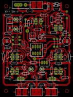
kypton v progress
Almost as bad as the "spooky".
Almost gave up on it. -- HULK SMASH FILTHY DIYA AMP !! 😀😀
Sort of redesigned it ...as I almost "gave up on it" .
.
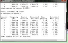
Came up with a deluxe VFA that will please even the guru's.
20hz - .5ppm
200hz - .5ppm
2k- 1ppm
10k - 3ppm
20k-4ppm
220V/uS slew ..
Good enough for me !
Servo'ed it (of course).
Had to use EVERY sq. CM of the board (85 parts).
Even thermally compensated the CCS and referenced the servo from
the lifted ground (not G2).
We have a "lab amp" here. 😀
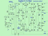
New schema and I will release the artwork tomorrow. (GLA lovers rejoice) !
This is the new "champ" (3)
This will be the last 😱 VFA contribution to this thread.
Next is the "eyesee" , a CFA IC based design.
OS
Almost as bad as the "spooky".
Almost gave up on it. -- HULK SMASH FILTHY DIYA AMP !! 😀😀
Sort of redesigned it ...as I almost "gave up on it"
.Came up with a deluxe VFA that will please even the guru's.
20hz - .5ppm
200hz - .5ppm
2k- 1ppm
10k - 3ppm
20k-4ppm
220V/uS slew ..
Good enough for me !
Servo'ed it (of course).
Had to use EVERY sq. CM of the board (85 parts).
Even thermally compensated the CCS and referenced the servo from
the lifted ground (not G2).
We have a "lab amp" here. 😀
New schema and I will release the artwork tomorrow. (GLA lovers rejoice) !
This is the new "champ" (3)
This will be the last 😱 VFA contribution to this thread.
Next is the "eyesee" , a CFA IC based design.
OS
Attachments
As most of the high performers, it's got its "character". But as soon as you manage to take it under control - it really flies 😎
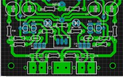
Nice one-sided PCB by the way
- Home
- Amplifiers
- Solid State
- Slewmaster - CFA vs. VFA "Rumble"