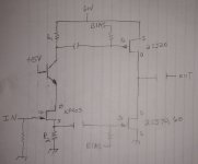
Thanks for the inputs. I did not know that KP901 is not a JFET. Knowing that, the original schematic with a KP903 with a cascode would suffice at 60V.
I ordered some of KP901 and KP902 to measure and evaluate.
The original schematic has a current source in series with the 2SJ20. The resistor is just to simplify.
KP902 appears to work to 50V Vds.
I ordered some of KP901 and KP902 to measure and evaluate.
The original schematic has a current source in series with the 2SJ20. The resistor is just to simplify.
KP902 appears to work to 50V Vds.
Pa sez that a current source doesn't really count as an active stage, so it would still be a two-transistor circuit. 🙂
You may also want to take a look at Vfet 2SK98/2SJ38 GB and e-pray item Transistor silicon 2P926B (KP926B) USSR Lot of 1 pcs.... I ordered some ...
You may also want to take a look at Vfet 2SK98/2SJ38 GB and e-pray item Transistor silicon 2P926B (KP926B) USSR Lot of 1 pcs.
There are some KP926B on the way to me. Thank you for the other link.
Pa sez that a current source doesn't really count as an active stage..
Constant current sources and cascodes. Darlingtons are two stages.....
😛
Just two transistors. A non-inverting DIY SIT-1. The KP901 is rated at 70V Vds and 20W dissipation from the data I have.
Hello woofertester. The schematic in your post above suggested that "IF" KP901 was instead a cascoded and tweaked J112, you have therein a built-in H2 generator; because Vgs=0 like taught by Mr. Pass.
Best
Anton
and you'r right ...... КП901 is a mosfet
maybe this could be handy
hmmmmmmm.... I will want to see Vds-Id curves for Vgs <<-1v It looks SIT-ish to me down there.
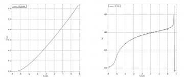
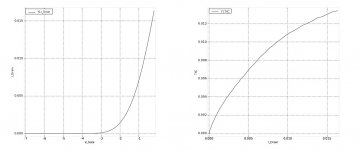
KP903 curves
Interesting family of curves for the KP903. From top to bottom, Vgs = +1, 0, -1, -2, -3.
This device is not happy at Vgs = +1V. Running the Vgs - Id curve reveals that the device saturates at Vgs = +0.8v. This device will require some degeneration to place it in its linear range. It looks pretty happy at Id = 300mA.
Attachments

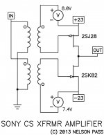
Maybe you will recall this one from BAF 2013:
Thank you for the suggestion. I will give that a try. There is a box of Edcor transformers in my stash. I just watched your BAF 2013 video. Interesting that the devices do not need to be isolated from a common heatsink for lashing this up.
and you'r right ...... КП901 is a mosfet
maybe this could be handy
The table consists mainly normally off SIT's called BSIT's near bjt behaviour. There are real ones like audio КП801 and switch mode К(2)П802 and К(2)П926. There might be some exotic staff like 2П985-X. As far as I know most of them if not all were designed by the very same guy at different fabs during country's self-destruction. Most SITs were from Novosibirsk Fab almost "@" logo, which used to be a vacuum tube plant.
Beware 926 or ОП-15 or 802 do have huge spread/variations in current and/or cut-off voltage so one need quite a few of them to get a match. Capacitances are quite big as well.
Cheers
I notice that the original schematic as drawn , will place +60V on the gate of the SIT .if the tube's heater is not pre-heated at the power on of the output stage B+ . May as well just use a mosfet follower output stage if using a triode front end
316a
316a
The table consists mainly normally off SIT's called BSIT's near bjt behaviour. There are real ones like audio КП801 and switch mode К(2)П802 and К(2)П926. There might be some exotic staff like 2П985-X. As far as I know most of them if not all were designed by the very same guy at different fabs during country's self-destruction. Most SITs were from Novosibirsk Fab almost "@" logo, which used to be a vacuum tube plant.
Beware 926 or ОП-15 or 802 do have huge spread/variations in current and/or cut-off voltage so one need quite a few of them to get a match. Capacitances are quite big as well.
Cheers
Thank you for this information. It helps quite a lot.
I notice that the original schematic as drawn , will place +60V on the gate of the SIT .if the tube's heater is not pre-heated at the power on of the output stage B+ . May as well just use a mosfet follower output stage if using a triode front end
316a
Yes agreed. Heater and bias supplies on first. Last on B+
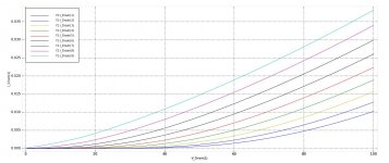
Some tubes and some tube sockets have arrived. ZM's recommendation of 6DJ8 is attached. Ignore the Axis labels. The curves are plate voltage, plate current, grid voltage, etc. Transconductance is delta I plate / delta V grid.
The curves span from Vg = 0 to Vg = -2.0 in equal steps.
For 60V, biasing at 10mA looks good. Transconductance at 60V at 10mA bias is a shade under 11 mA / volt.
Paralleling both sections would give 20mA bias and 22 mA / V transconductance.
The curves span from Vg = 0 to Vg = -2.0 in equal steps.
For 60V, biasing at 10mA looks good. Transconductance at 60V at 10mA bias is a shade under 11 mA / volt.
Paralleling both sections would give 20mA bias and 22 mA / V transconductance.
Attachments
- Home
- Amplifiers
- Pass Labs
- SIT-Triode Hybrid idea