Dear All
After building the very good sounding HDRP200 explained here:
HDRP200 High speed very low distortion singleton power amplifier
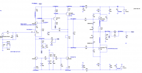
I wanted to try the same simple design but using a Jfet input and omit the input capacitor.
In this new amp I am using a ccs to set the operation current of the IPS jfet and the offset control depends on this ccs stability.
The IPS is now loaded by a resistor R3 (390ohms).
The transimpedance stage (VAS) is buffered and drives directly the output lateral mosfets.
This amp sounds fast, providing a very detailed low end.
Will now finetune it because I feel treble can be ameliorated.
Here you have the working circuit:
After building the very good sounding HDRP200 explained here:
HDRP200 High speed very low distortion singleton power amplifier
I wanted to try the same simple design but using a Jfet input and omit the input capacitor.
In this new amp I am using a ccs to set the operation current of the IPS jfet and the offset control depends on this ccs stability.
The IPS is now loaded by a resistor R3 (390ohms).
The transimpedance stage (VAS) is buffered and drives directly the output lateral mosfets.
This amp sounds fast, providing a very detailed low end.
Will now finetune it because I feel treble can be ameliorated.
Here you have the working circuit:
Attachments
Last edited:
now I want to upgrade the input CCS with a cascoded jfet as I believe that if I use a matched NJfet for this purpose and thermally couple it with the input device I can significantly reduce offset variations.
I did not try this new configuration and hope to have sufficient input here to arrive at a good final solution.
If there is enough interest I can also provide LTSPICE simulations.
I did not try this new configuration and hope to have sufficient input here to arrive at a good final solution.
If there is enough interest I can also provide LTSPICE simulations.
Attachments
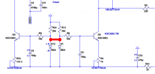
Why not install the red wire? It eliminates one resistor and perhaps one LED.
_
Thank you for your input.
Indeed I can simplify this design and use only one LED to reference both CCS but this way the IPS CCS will be modulated by the signal passing in the VAS CCS.
Would you care to have a look at the jfet CCS ?
I want to bond the jfet CCS with the IPS Jfet in order to minimize offset current variations.
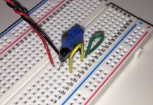
Just finished a jfet ccs in a breadboard and it works ")
Hope it tracks temp well when the jfets are termaly bonded.....
Once I read that the major offset fluctuations come from temp differences in the VAS... Instead I am trying to limit fluctuations acting in the IPS.... hope it works ok
Hope it tracks temp well when the jfets are termaly bonded.....
Once I read that the major offset fluctuations come from temp differences in the VAS... Instead I am trying to limit fluctuations acting in the IPS.... hope it works ok
With regard to C6 and C9. Fifty years ago when playing with the ccs that used a pair of 1n4148 diodes I too tried a bypass cap. My ears didn't notice any improvement by using a 220uf electrolytic cap but I did notice a little improvement when I used a rather cheep 1.5uf mylar cap. Hay 50 years ago exotic caps were rather hard to find. If I was trying this again I might be tempted to use something like a 50uf Silk II with a small bypass cap.
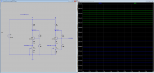
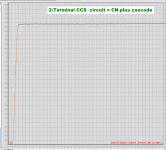
It's possible to get a plot of the Current vs. Voltage behavior of an actual constant current sink in real life, made with real components (not simulated). Just hook it up to a semiconductor curve tracer and run a sweep test, as though it were a Zener diode. CCS+ goes to the ZDCathode pin of the curve tracer, CCS- goes to the ZDAnode pin of the curve tracer. The CCS circuit is on a little piece of solderless breadboard. Photo 1 below shows a J113 JFET with a trimmer potentiometer in series with the source leg. The red and black wires connect the CCS to the curve tracer.
Figure 2 shows an example I-V output, made by the LockyZ curve tracer. The horizontal axis is voltage across the CCS, from 0V to 20+ volts. The vertical axis is current through the CCS, from 0 to 6.4 milliamps. The particular circuit tested here is Figure 30 of the LM334 datasheet. It consists of three components: an LM334, a single resistor (trimpot), and a JFET cascode device.
Plotting the actual, measured behavior of real circuits made from real components, means you are not forced to rely upon dodgy SPICE models, created by people you've never met, whose skill and ability you cannot know, working in a previous calendar century.
_
Attachments
Last edited:
C1/C11 are not needed.
It's better (cheaper) to change values of gate stoppers on them.
The idea is that RC=const (the same on upper/lower mosfet), where R is gate stopper value, and C is input capacitance of the mosfet (N/P has different capacitance, check in the sheets).
Sometimes you can see in other amps that upper gate stopper is 330 Ohm, and lower one 220 Ohm..
Last edited:
C1 & C11 are necessary? I have some very HF oscilation with Exicon laterals, so it might be a fix for me?
Regards
Laterals are tricky.... any inductance in the pub can start oscillations.
I cure this with small caps from gate to drain.
You can instead use 30pf caps only on the nmos....
But I prefer to use 15pf on all laterals.ý
I am using 100u normal el.... do you believe i should bypass those?With regard to C6 and C9. Fifty years ago when playing with the ccs that used a pair of 1n4148 diodes I too tried a bypass cap. My ears didn't notice any improvement by using a 220uf electrolytic cap but I did notice a little improvement when I used a rather cheep 1.5uf mylar cap. Hay 50 years ago exotic caps were rather hard to find. If I was trying this again I might be tempted to use something like a 50uf Silk II with a small bypass cap.
Thank you so much.... Will try that asapIt's possible to get a plot of the Current vs. Voltage behavior of an actual constant current sink in real life, made with real components (not simulated). Just hook it up to a semiconductor curve tracer and run a sweep test, as though it were a Zener diode. CCS+ goes to the ZDCathode pin of the curve tracer, CCS- goes to the ZDAnode pin of the curve tracer. The CCS circuit is on a little piece of solderless breadboard. Photo 1 below shows a J113 JFET with a trimmer potentiometer in series with the source leg. The red and black wires connect the CCS to the curve tracer.
Figure 2 shows an example I-V output, made by the LockyZ curve tracer. The horizontal axis is voltage across the CCS, from 0V to 20+ volts. The vertical axis is current through the CCS, from 0 to 6.4 milliamps. The particular circuit tested here is Figure 30 of the LM334 datasheet. It consists of three components: an LM334, a single resistor (trimpot), and a JFET cascode device.
Plotting the actual, measured behavior of real circuits made from real components, means you are not forced to rely upon dodgy SPICE models, created by people you've never met, whose skill and ability you cannot know, working in a previous calendar century.
_
Laterals are tricky.... any inductance in the pub can start oscillations.
I cure this with small caps from gate to drain.
You can instead use 30pf caps only on the nmos....
But I prefer to use 15pf on all laterals.ý
Thanks, will try that.
Regards
Interesting design. A couple of comments - the VAS pair have a rather low bias resistor of only 390 ohms. Given the emitter resistor of the VAS is 22 that limits the gain of the stage considerably.
Would be worth considering an active load (current mirror with the reference arm driven by the same current as in the FET). I've used that idea a long time ago and Kokoriantz did it for his version of the JLH 10W.
I recommend keeping the CCS for the input stage and VAS on separate bias chains, and not coupling them. In fact that separation should be done oin Self's Blameless too. Combining the two lends itself for modulating the VAS or input stage current by the other stage. Near clipping particularly, a single bias could disrupt the circuit. Self separated the VAS and input stage with a 1k resistor but that slows down the VAS transistor. Not recommended to combine the two diodes. Cost of a resistor and LED or so is a small expense for a hifi design.
- Status
- This old topic is closed. If you want to reopen this topic, contact a moderator using the "Report Post" button.
- Home
- Amplifiers
- Solid State
- Singleton Jfet Input with laterals.... very fast amp