about hip4080a ,please help
Recently I designd a digitl amplifier ,the sch and pcb is DPA-1KWB.pdf,i have changed the mosfet to ifrb23n15d and the input
triangle wave used wave generator ,when i test it ,the feedback was open-loop,
the problem is when i used 20v vcc on the mosfet,the chip IC hip4080 was burned,and I don't kown that why?
i'm sorry my english was very poor.
Attachments
Hello Cromaniac ...
Very nice project. After i read this thread i started wondering if it is possible to use this topology with 2 pieces of IR2110 instead of the Intersil chip.
The advantage would be that you can use it with almost 200Vdc thus reaching higher power.
I am now in the proces of simulating such a contraption in LTSpice but i have problems because i do not have the serious knowhow needed for designing such an amp.
The simulation does not give the power output that i was hoping for and has big of THD.
Another problem is that the sinewave is all crooked, witch makes me think that the feedback part is not ok and also the gain (input part) has some problems.
Mine uses LT1016 fast comparator and 2 pieces of IR2110 in fulbridge configuration, 4 pieces of IRFB4227 transistors and 180Vdc single supply for the power stage, 15Vdc for the IR drivers and the LT comparator.
I wold realy apreciate if you guys could help me make this thing stable. I have a lot to learn from this BTL topology.
Best regards,
Savu Silviu
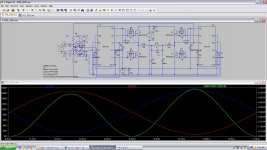
Made it work.
RMS Power is 3.1KW
THD is 1.01%
2Vpp 1Khz sine
sw freq is 1.2Mhz (don't understand why)
it still needs a lot of tweaks but the future of this looks promissing
Best Regards,
Savu Silviu
RMS Power is 3.1KW
THD is 1.01%
2Vpp 1Khz sine
sw freq is 1.2Mhz (don't understand why)
it still needs a lot of tweaks but the future of this looks promissing
Best Regards,
Savu Silviu
Attachments
Last edited:
In your schematic................
Your feedback is taken before filter, whereas UCD is post filter feedback type, change the feedback to after filter. Also the feedback network is missing essential components to form a UCD type amp.
Your feedback is taken before filter, whereas UCD is post filter feedback type, change the feedback to after filter. Also the feedback network is missing essential components to form a UCD type amp.
Thanks for the observation Workhorse.
I will look at it this night. So i will change the feedback node and also i will correct the feedback. Hope it will work this could turn out to be a really nice amp.
Best Regards,
Savu Silviu
I will look at it this night. So i will change the feedback node and also i will correct the feedback. Hope it will work this could turn out to be a really nice amp.
Best Regards,
Savu Silviu
any good advice regarding the feedback? because i never designed buteworth filters or any filter 😛.
If you have a link to an application note or something it would help me a lot.
Thanks again ΚΔΠШΔЯ
If you have a link to an application note or something it would help me a lot.
Thanks again ΚΔΠШΔЯ
This document has some basic info on ucd topology:
http://www.hypex.nl/docs/ucd_aes.pdf
You'll have to experiment with values in phase-lead network until you get to desirable switching frequency and performance.
For start, try with values I used in my schematic.
http://www.hypex.nl/docs/ucd_aes.pdf
You'll have to experiment with values in phase-lead network until you get to desirable switching frequency and performance.
For start, try with values I used in my schematic.
hi savu
greetings nice amp is it possible for me to make this amp did you assemble it
on double sided pcb first d class ended in faliure guess have to keep on trying is it possible
to make this circuit
thanking you
andrew lebon
greetings nice amp is it possible for me to make this amp did you assemble it
on double sided pcb first d class ended in faliure guess have to keep on trying is it possible
to make this circuit
thanking you
andrew lebon
Hello Andrewlebon,
it should be. the idea is that this will certainly need dual layer with thick groundplane, shileded output inductors, wery thick and short traces on the power stage, a very good layout with everithing positioned close together, a serious power supply very well filtered, balanced input, and so on.
But remember. this is only a simulation, i have never built it. i only finished simulating it some hours ago. it has no protection circuits what so ever.
you could try to build it for lower power levels.
after i am donne tweaking it i will post the last version of schematic and work on a layout.
Best regards,
Savu Silviu
hi savu
greetings thanks for your reply will wait for your schematic thanks and hope your
project is a success
thanking you
andrew lebon
greetings thanks for your reply will wait for your schematic thanks and hope your
project is a success
thanking you
andrew lebon
I have to wait from some feedback from the people on the forum that have experience and knowhow. i am nube in this matter. i was amazed that i was able to make this as a simulation. the schematic is made from different parts of class d amps that i found on the forum. i am still searching for a schematic of a differential output opamp input stage.
Best regards,
Savu Silviu
Best regards,
Savu Silviu
any good advice regarding the feedback? because i never designed buteworth filters or any filter 😛.
If you have a link to an application note or something it would help me a lot.
Thanks again ΚΔΠШΔЯ
Have a look at this thread:-
http://www.diyaudio.com/forums/class-d/85389-philips-ucd-application-note.html
Have a look at this thread:-
http://www.diyaudio.com/forums/class-d/85389-philips-ucd-application-note.html
hello Workhorse, i have studied it last night for a bit. i have done it.
the simulation works with great results.
please take a look at the schematic . it is some posts up.
thanks a lot
Savu Silviu
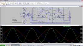
Hello Cromaniac ...
I folowed your advice and Konwars advice. The results are Quite nice.
RMS power into 4 Ohm is 4KW at 190Vdc with 1.17 % THD, 420Khz SW FQ, fed with 2Vpp at 1Khz.
Schematic attached ...
Hello savu,
I noticed that oscillation is not symmetric when output approaching the two rails in the simulation. I don't know whether it should be or should not be.
Cheers,
Hello savu,
I noticed that oscillation is not symmetric when output approaching the two rails in the simulation. I don't know whether it should be or should not be.
Cheers,
Oops! I have checked the wrong trace which is the power trace. The output trace is symmetric actually.
- Status
- Not open for further replies.
- Home
- Amplifiers
- Class D
- Single supply bridge UcD, referencing the signals