I did some more measuring. I hooked up my signal generator, an old HP 3310A, and an oscilloscope to the amplifier to check the clipping voltage, and to check the frequency response. Just for fun I also looked at some square waves.
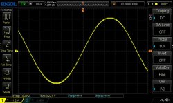
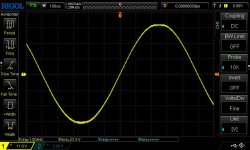
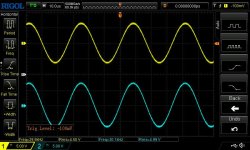
The amplifier sine output seemed to start to deform at around 65W or so, and flattening of the waveform was quite obvious at 70W.
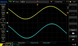
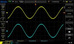
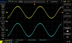
To check the frequency response I monitored the input and output sine wave signal levels, with the input level shown by the yellow oscilloscope trace and the output level shown by the blue oscilloscope trace. The input level was kept at 5Vrms. The output level was typically around 4.47Vrms. The high frequencies appeared to be slightly boosted, measured at 4.50Vrms, and extended to at least 30kHz. At the bottom end the 30Hz output was still 4.47Vrms, and 20Hz was 4.40Vrms. Using this equation for expressing the difference in voltage as dB:
dB = 20 log (V2/V1)
At 20Hz the decrease in output level was: 20 log (4.40V/4.47V) = -0.14dB
So the amplifier frequency response measured quite well.
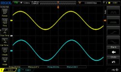
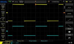
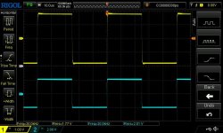
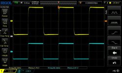
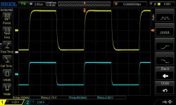
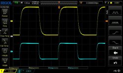
The square waves showed no surprises because of the amplifier's extended high frequency response. At high frequencies, an overshoot is seen at the edge of the waveform. I think that is due to the slight elevation of the high frequencies.
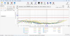
I also hooked up the Focusrite/REW FFT rig and did a sweep with the DIY FE2022 providing voltage gain to the signal. The amplifier was measured at 1W output into 8 Ohm. Second harmonic distortion dominated and was constant throughout the audio frequency range.
The amplifier sine output seemed to start to deform at around 65W or so, and flattening of the waveform was quite obvious at 70W.
To check the frequency response I monitored the input and output sine wave signal levels, with the input level shown by the yellow oscilloscope trace and the output level shown by the blue oscilloscope trace. The input level was kept at 5Vrms. The output level was typically around 4.47Vrms. The high frequencies appeared to be slightly boosted, measured at 4.50Vrms, and extended to at least 30kHz. At the bottom end the 30Hz output was still 4.47Vrms, and 20Hz was 4.40Vrms. Using this equation for expressing the difference in voltage as dB:
dB = 20 log (V2/V1)
At 20Hz the decrease in output level was: 20 log (4.40V/4.47V) = -0.14dB
So the amplifier frequency response measured quite well.
The square waves showed no surprises because of the amplifier's extended high frequency response. At high frequencies, an overshoot is seen at the edge of the waveform. I think that is due to the slight elevation of the high frequencies.
I also hooked up the Focusrite/REW FFT rig and did a sweep with the DIY FE2022 providing voltage gain to the signal. The amplifier was measured at 1W output into 8 Ohm. Second harmonic distortion dominated and was constant throughout the audio frequency range.
Attachments
-
 66W.jpg68 KB · Views: 80
 -
 68W.jpg68.1 KB · Views: 64
 -
 Clipping 70W.jpg67.9 KB · Views: 56
 -
 Sine 20.jpg68.6 KB · Views: 57
 -
 Sine 30.jpg69.5 KB · Views: 50
 -
 Sine 1k.jpg72.2 KB · Views: 49
 -
 Sine 20k.jpg72.2 KB · Views: 54
 -
 Sine 30k.jpg75.4 KB · Views: 64
 -
 Square 10k.jpg63.4 KB · Views: 64
 -
 Square 20k.jpg63.5 KB · Views: 63
 -
 Square 50k.jpg64.7 KB · Views: 65
 -
 Square 100k.jpg65.7 KB · Views: 61
 -
 Square 200k.jpg66.7 KB · Views: 85
 -
 THF-51S MuFF 75VDC PS DIY FE2022 8R 1W.jpg212 KB · Views: 83

Hi, I’ve been following this tread for a while now and I’m slowly gathering the parts to build two monoblocs. I have a question regarding the power transformer : I’m buying some new antek for this project and I’m wondering what is best, two secondary in series or two secondary in parallel? I’ve read somewhere that when paralleling two secondary they have to be exactly the same or there may be some humming. Thank you!
Hubert
Hubert
Yes, they have to be identical in every way. If not the two secondaries may not share the load equally resulting in abnormal currents and overload.
However if each secondary has its own bridge rectifier and the DC from each rectifier is paralleled, then there is no problem.
So bottom line, it is possible to parallel connect two secondaries but if you are unsure whether the two secondaries are exactly identical, add the extra bridge rectifier.
Or go with half the voltage and series connect the secondaries.
Sometimes when choosing transformers, other factors such as extra low voltage secondary windings may sway your decision. For instance if the transformer requiring parallel secondaries has extra lower voltage winding that you need but the transformer requiring series secondaries does not have the extra lower voltage winding that you need, it may be less expensive and less complicated to go with the parallel secondaries with the extra low voltage secondaries and add the bridge rectifier rather than go with the series secondaries and then have to add transformer(s) for the low voltage.
Hi
In regards to above post 757, what if I’d like to use N channel for the puck M1, would I require lots of changes to the circuit? I already have a few N channel powerful MOSFET and would rather spend that $100 on something else I don’t already have.
Thanks
Eric
In regards to above post 757, what if I’d like to use N channel for the puck M1, would I require lots of changes to the circuit? I already have a few N channel powerful MOSFET and would rather spend that $100 on something else I don’t already have.
Thanks
Eric
An N channel mosfet can be used in a mu follower follower. However the circuit would require changes. For instance Nelson's Sony DIY VFET OS2 amplifier is a mu follower follower that uses an N channel SIT and an N channel mosfet. Note that R1 and R2 in the DIY VFET OS2 circuit are the equivalent of R2 and R13 in my LTSpice circuit in post #757.

Attachments
Last edited:
That is the problem, I’m not sure it would be done correctly…and I believe I would not be able to use your PCB.
I have been listening to the amps for a bit now - left channel revised with 75V power supply and right channel with the original 62V power supply. I am quite happy with the sound so onward with more DIYing - playing with LTSpice and KiCad. For me both programs are entertaining, educating, and brain teasing.
As I mentioned in post #723 I want to try the circuit with the SIT bias voltage applied to the gate of an input buffer. I do not know whether changes will improve the sound of the amp or not but I am a DIYer who wants to explore. Zen Mod applied the SIT bias voltage to the gate of an input buffer in his series of Singing Bush amplifiers so I want to give it a try. I had already done that with a common source THF-51S output stage (https://www.diyaudio.com/community/...r-revisited-with-feedback.408193/post-7575917) but I want to try it with a common drain output stage. Currently the SIT bias voltage is applied directly to the SIT gate through a gate leak resistor. If the SIT has high gate leak current, the gate leak current will draw down the bias voltage resulting in possible runaway SIT idle current. Fortunately none of my THF-51S has high enough gate leak current for it to be a problem but there are some THF-51S that may be problematic. I did have one 2SK180 in a choke loaded single ended amplifier that was a problem. The idle current would increase as the amp warmed up and despite adjustment to the bias current on the fly, the idle current would not stabilize. I finally gave up and replaced the 2SK180.
The SITs also have high input capacitance so low output impedance of the preamp feeding the SIT amp is necessary to maintain good high frequency response. An input buffer would allow a preamp with high output impedance to be used with the amp and not suffer a loss of high frequency. My preamps have low output impedance so that is not a problem but an input buffer on the amplifier would allow for flexibility in preamp choice.
My plan for the input buffer is a constant current source (CCS) loaded JFET or mosfet. For this 75VDC power supply version of the amplifier, I have chosen the DN2540 mosfet in the TO-92 package for both the CCS and buffer. I have used the DN2540 as a buffer in Michael Rothacher's Luminaria preamp design and also in my 2SK79 preamp. It can handle the high power supply voltage whereas JFETs such as the SK170 or J113 cannot, unless they are cascoded. I want to keep my circuit simple.
To establish the baseline performance of the amplifier with no input buffer, I ran an LTSpice simulation. The goal was to establish a workable circuit that did not compromise power output. Here are the baseline results for the amplifier with no input buffer. The power supply was -75V, current 3A, input signal(red trace) was 38Vp, output signal (green trace) was about 34Vp at 8 Ohm speaker load. This worked out to 72W output power. This was the maximum voltage output of the amplifier at onset of clipping. The signal at the SIT gate was the blue trace.


The next amplifier circuit simulated was the amplifier with the DN2540 buffer at the amplifier input, and with the SIT bias voltage applied at the DN2540 gate. The power supply voltage and current and signal input voltage were kept as in the previous simulation, and will also be kept for subsequent circuits/simulations.
The voltage plots showed for the same 38Vp input signal voltage, the signal negative peak at the output of the buffer/input of SIT was clipped. Looking at the plot, the signal can be seen to be truncated at about -75V, which was also the power supply voltage. So it was apparent that the SIT bias voltage applied to the audio signal at the buffer gate caused the signal at the buffer output to be clipped. This truncated signal then went through the SIT and out to the speaker. The result was a clipped output stage signal.
The circuit was not capable of outputting a good 38Vp audio signal because the SIT bias/input buffer circuit clipped the signal before it went to the output stage.


The next circuit is the same as the previous circuit but with the input audio signal voltage reduced, the output sine wave from the buffer was no longer clipped. The buffer input signal was 35Vp and the THF-51S output stage signal was about 31Vp. This worked out to 60W. Compared to the 72W from the circuit with no input buffer, the input buffer cost the amplifier 12W. The THF-51S output stage was capable of outputting 72W but the buffer stage was not able to provide the necessary signal voltage.


To restore the signal voltage at the THF-51S gate back to the original 38Vp, the power supply voltage to the buffer circuit must be increased by the THF-51S bias voltage that was applied to the input of the buffer. The original circuit showed that the THF-51S Vgs was approximately 3V. In the following simulation the power supply voltage to the buffer stage was increased by that 3V to offset the effect of the bias voltage on the buffer input signal buffer. As can be seen on the signal voltage plots, the full power output of the amplifier was restored.


Because Tokin SIT Vgs varies greatly from sample to sample, I will add -15VDC to the -75VDC power supply to provide a total of -90VDC to power the DN2540 buffer circuit. That should be more than enough voltage to account for all SIT Vgs possibilities.
As I mentioned in post #723 I want to try the circuit with the SIT bias voltage applied to the gate of an input buffer. I do not know whether changes will improve the sound of the amp or not but I am a DIYer who wants to explore. Zen Mod applied the SIT bias voltage to the gate of an input buffer in his series of Singing Bush amplifiers so I want to give it a try. I had already done that with a common source THF-51S output stage (https://www.diyaudio.com/community/...r-revisited-with-feedback.408193/post-7575917) but I want to try it with a common drain output stage. Currently the SIT bias voltage is applied directly to the SIT gate through a gate leak resistor. If the SIT has high gate leak current, the gate leak current will draw down the bias voltage resulting in possible runaway SIT idle current. Fortunately none of my THF-51S has high enough gate leak current for it to be a problem but there are some THF-51S that may be problematic. I did have one 2SK180 in a choke loaded single ended amplifier that was a problem. The idle current would increase as the amp warmed up and despite adjustment to the bias current on the fly, the idle current would not stabilize. I finally gave up and replaced the 2SK180.
The SITs also have high input capacitance so low output impedance of the preamp feeding the SIT amp is necessary to maintain good high frequency response. An input buffer would allow a preamp with high output impedance to be used with the amp and not suffer a loss of high frequency. My preamps have low output impedance so that is not a problem but an input buffer on the amplifier would allow for flexibility in preamp choice.
My plan for the input buffer is a constant current source (CCS) loaded JFET or mosfet. For this 75VDC power supply version of the amplifier, I have chosen the DN2540 mosfet in the TO-92 package for both the CCS and buffer. I have used the DN2540 as a buffer in Michael Rothacher's Luminaria preamp design and also in my 2SK79 preamp. It can handle the high power supply voltage whereas JFETs such as the SK170 or J113 cannot, unless they are cascoded. I want to keep my circuit simple.
To establish the baseline performance of the amplifier with no input buffer, I ran an LTSpice simulation. The goal was to establish a workable circuit that did not compromise power output. Here are the baseline results for the amplifier with no input buffer. The power supply was -75V, current 3A, input signal(red trace) was 38Vp, output signal (green trace) was about 34Vp at 8 Ohm speaker load. This worked out to 72W output power. This was the maximum voltage output of the amplifier at onset of clipping. The signal at the SIT gate was the blue trace.
The next amplifier circuit simulated was the amplifier with the DN2540 buffer at the amplifier input, and with the SIT bias voltage applied at the DN2540 gate. The power supply voltage and current and signal input voltage were kept as in the previous simulation, and will also be kept for subsequent circuits/simulations.
The voltage plots showed for the same 38Vp input signal voltage, the signal negative peak at the output of the buffer/input of SIT was clipped. Looking at the plot, the signal can be seen to be truncated at about -75V, which was also the power supply voltage. So it was apparent that the SIT bias voltage applied to the audio signal at the buffer gate caused the signal at the buffer output to be clipped. This truncated signal then went through the SIT and out to the speaker. The result was a clipped output stage signal.
The circuit was not capable of outputting a good 38Vp audio signal because the SIT bias/input buffer circuit clipped the signal before it went to the output stage.
The next circuit is the same as the previous circuit but with the input audio signal voltage reduced, the output sine wave from the buffer was no longer clipped. The buffer input signal was 35Vp and the THF-51S output stage signal was about 31Vp. This worked out to 60W. Compared to the 72W from the circuit with no input buffer, the input buffer cost the amplifier 12W. The THF-51S output stage was capable of outputting 72W but the buffer stage was not able to provide the necessary signal voltage.
To restore the signal voltage at the THF-51S gate back to the original 38Vp, the power supply voltage to the buffer circuit must be increased by the THF-51S bias voltage that was applied to the input of the buffer. The original circuit showed that the THF-51S Vgs was approximately 3V. In the following simulation the power supply voltage to the buffer stage was increased by that 3V to offset the effect of the bias voltage on the buffer input signal buffer. As can be seen on the signal voltage plots, the full power output of the amplifier was restored.
Because Tokin SIT Vgs varies greatly from sample to sample, I will add -15VDC to the -75VDC power supply to provide a total of -90VDC to power the DN2540 buffer circuit. That should be more than enough voltage to account for all SIT Vgs possibilities.
I’m running the Buffer at the input and it sounds great and the bias is much more stable on the sit. Thanks for the analysis 😀👍
Oh don’t forget a Zener across the DN2540 input. I lost a pair with a lightning strike not far from my home.
My current amp without input buffer is stable so it has not been an issue for me. I am trying a buffer just for the fun of it. I'm just a amateur diyer so this is all an experiment, a learning experience, and an exercise for the brain. 🤓
I haven't included a zener at the DN2540 in my previous builds (Luminaria and 2SK79 preamps) but then lightning strikes here are very rare.
I haven't included a zener at the DN2540 in my previous builds (Luminaria and 2SK79 preamps) but then lightning strikes here are very rare.
most dangerous lightning strikes around here are those - in between my ears
so, zeners are mandatory for my concoctions

so, zeners are mandatory for my concoctions
Well I find your amateur commentary most insightful. Keep cooking Chef Mah.I'm just a amateur diyer so this is all an experiment, a learning experience, and an exercise for the brain. 🤓
I get brain zap sometimes just before I fall asleep. It feels like an electrical jolt in the brain💥⚡💥⚡💥
May I need a zener implant. 🤓
May I need a zener implant. 🤓
Happy New Year!
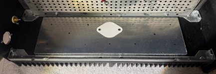
Goods have arrived - thanks Ben for the Gerber files.
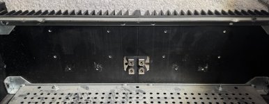
My idea is to reuse the M3 screw holes from Aleph J for mounting the 8mm aluminum plate on one side (with 2 extra holes for IXTN).
The screw layout for SIT is shown in the attached picture (M4 screws to be used).
I want to use a thin layer of thermal compound between heat sink and aluminum plate.
I have a thermal pad for SIT and for IXTN I will just use thermal paste or pad like that https://a.co/d/5vdcCKZ .
Any comments are welcome.
Goods have arrived - thanks Ben for the Gerber files.
My idea is to reuse the M3 screw holes from Aleph J for mounting the 8mm aluminum plate on one side (with 2 extra holes for IXTN).
The screw layout for SIT is shown in the attached picture (M4 screws to be used).
I want to use a thin layer of thermal compound between heat sink and aluminum plate.
I have a thermal pad for SIT and for IXTN I will just use thermal paste or pad like that https://a.co/d/5vdcCKZ .
Any comments are welcome.
Attachments
- Home
- Amplifiers
- Pass Labs
- Single Ended Tokin SIT THF-51S Common Drain Mu Follower Amplifier, 45W?