R1 is 6R8. All values are like this
http://www.diyaudio.com/forums/attachment.php?s=&postid=1722356&stamp=1232753798
except for the zener that I use, 1n4759a.
http://www.diyaudio.com/forums/attachment.php?s=&postid=1722356&stamp=1232753798
except for the zener that I use, 1n4759a.
The first version was wrong, the latest pdf should have been fixed. I based the pcb on the ltspice schematic, so the parts numbers are slightly different. R1 on your schematic is R3 on mine. This should be a lesson for me to make an effort to keep the parts numbered as the author did.
ikoflexer said:except for the zener that I use, 1n4759a.
I see on Zener PDF online that 4759A = 62V! 4749A=24V.
ikoflexer said:The first version was wrong, the latest pdf should have been fixed. I based the pcb on the ltspice schematic, so the parts numbers are slightly different. R1 on your schematic is R3 on mine. This should be a lesson for me to make an effort to keep the parts numbered as the author did.
Naah! No worries...if its where it should be, no problemo.
salas said:
I see on Zener PDF online that 4759A = 62V! 4749A=24V.
My mistake, I meant 4749. I will just redo it point to point with fresh parts.
Yes, just do that. Its working for many people. When it will work OK for you too, then you can find the board's culprit at your leisure.

salas said:
Nice. Did you populate the board yet?
Hi Salas
I did not populate the board yet because I need to figure out some details. I have been checking the pcb and everything seems ok regarding the mosfets and NPN.
I can not figure out where Drain and Source are on the 2SK170 in your design

Are Drain and Gate connected together ? If so the Source connects to R4...
Ricardo
Nico,nicoch46 said:I don't use main earth
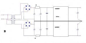
B only suits a single rectifier and the Shunts must be a +ve & -ve pair.
A is OK with dual rectifiers and OK with a pair of +ve shunts or mixed +ve & -ve shunts or a pair of -ve shunts.
The resistors marked ? should be 0r0.
There was a thread suggesting that Inductors in the returns would work better, but I cannot recall the conclusion.
Hi,
for these Nchannel jFETs the Drain is the more positive connection and the Source is the more negative connection, i.e. D @ Top and S @ Bottom.
However, most jFETs are made such that they are truly symmetrical, i.e. one can swap D & S without affecting performance.
When the Gate is connected to Source, the jFET operates as a CCS and passes Idss from Drain to Source. It will try to operate over the range of ~ Pinch Off voltage to Vdsmax.
But watch dissipation of high Idss devices with high Vds. They will overheat to destruction. A gr with 25Vds and passing 3mA, dissipates 75mW<<400mW Pdmax.
A v device with 20Vds and passing 15mA dissipates 300mW and this will overheat the junction if Ta>=50degC.
Thank you Andrew TAndrewT said:Hi,
for these Nchannel jFETs the Drain is the more positive connection and the Source is the more negative connection, i.e. D @ Top and S @ Bottom.
However, most jFETs are made such that they are truly symmetrical, i.e. one can swap D & S without affecting performance.
So If I get it wright, in Salas schunt we have G and S connected together (Q5)
In my pcb I have D and G connected together... must I invert the connections ?
Ricardo
RCruz said:
Thank you Andrew T
So If I get it wright, in Salas schunt we have G and S connected together (Q5)
In my pcb I have D and G connected together... must I invert the connections ?
Ricardo
As you face 2SK170BL and you can read its type number you must connect the middle pin with the right pin. The free pin goes up as you read the schematic, the together ones connect down to the respective resistors that go to earth.
RCruz said:In my pcb I have D and G connected together... must I invert the connections ?
Ricardo
 Hmmm...can this be the bug that gave problems to Ikoflexer's shunt?
salas said:
🙁 could be, since the second regulator I built point to point still shows the same ripple on the output. I'll try hooking up the jfets as you say. I too thought they were symmetrical.
- Home
- Source & Line
- Analogue Source
- Simplistic NJFET RIAA