Salas,
I see many builders are using a low voltage device for M1.
M1 takes enormous stress at start up for a few us or ms depending on the load characteristics.
Is there a history or good, or poor, or bad, reliability for the M1 devices?
I see many builders are using a low voltage device for M1.
M1 takes enormous stress at start up for a few us or ms depending on the load characteristics.
Is there a history or good, or poor, or bad, reliability for the M1 devices?
Although it started as a what I had in the parts bin thing, very good M1 reliability. Seems that the small Vref filter cap (1uF) does not stress them long enough at start up.
Yes, there is only 1uF and 1uF+3r3 as a start up load inside the regulator.
What is the external load capacitance?
I will point out that I believe a lot of the good performance of these Salas Style regulators comes from the fact that very few capacitors are used.
What is the external load capacitance?
I will point out that I believe a lot of the good performance of these Salas Style regulators comes from the fact that very few capacitors are used.
I don't remember why that value, really. On the lower range circuit it was sub 1K indeed.
Its 4 years now that initial circuit and I arrived there on test, it wasn't simulated before.
*Few caps and no significant lytics was a a quality and economy goal.
**Maybe he needs an input decoupling film if he has got long wires.
Its 4 years now that initial circuit and I arrived there on test, it wasn't simulated before.
*Few caps and no significant lytics was a a quality and economy goal.
**Maybe he needs an input decoupling film if he has got long wires.
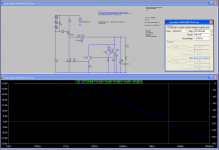
Just a question: as I see it, the collector of Q3 is kept at 1,2 volt.
Then I see a mismatch with the base of Q1 at [at least] 0,6 volt.
So maybe this design needs a darlington at Q1? on the other hand, this idea could work when using a NPN pair current source and proper termination at 'the top'..
apologies for a maybe stupid question.
Then I see a mismatch with the base of Q1 at [at least] 0,6 volt.
So maybe this design needs a darlington at Q1? on the other hand, this idea could work when using a NPN pair current source and proper termination at 'the top'..
apologies for a maybe stupid question.
No,
the collector of Q2 is @ ~ 1.3V below the output rail.
The base of Q1 is @ ~ 0.65V below the output rail. This forces Q3 to a Vce of <0.1Vce.
i.e. Q3 is saturated.
Not a good way to ensure good performance from a two transistor CCS. That CCS determines the current and thus the voltage drop across R9.
Your idea of a darlington for Q1, or maybe a mosFET, would help get Q3 Vce back up to at least 0.5V and maybe towards a couple of volts.
Last edited:
Make R10 4K7, see if its stabler.
Hi Salas,
The regulator is stable after making R10 as 4k7. Thanks!!! Q1 will now also dissipate less heat. Is there a drawback to this?
---
How hot does R9 become? Be careful it has a lot of volts across it !
AndrewT, it is not hot, only a little warm.
Regards,
-MW
eboz, nice. No problem, its better gain and less dissipation that way. I had revised that when I had used it near max Vo a long time ago, its 4k7 on the schematics from back then also. So you are at standard.
No,
the collector of Q2 is @ ~ 1.3V below the output rail.
The base of Q1 is @ ~ 0.65V below the output rail. This forces Q3 to a Vce of <0.1Vce.
i.e. Q3 is saturated.
Not a good way to ensure good performance from a two transistor CCS. That CCS determines the current and thus the voltage drop across R9.
Your idea of a darlington for Q1, or maybe a mosFET, would help get Q3 Vce back up to at least 0.5V and maybe towards a couple of volts.
There is the JFET Vref standard one, the SSHV1 one to make, instead of head scratching revising the initial idea one, although some still find synergistic qualities in it for some circuits and like it as is...
Triode asks a question and I give my thoughts in answering that question?
Why the "stop tinkering" statement?
Why the "stop tinkering" statement?
I did not make any statement, I reminded there is the evolution done already in one way, its open source you you do whatever.
There is the JFET Vref standard one, the SSHV1 one to make, instead of head scratching revising the initial idea one, although some still find synergistic qualities in it for some circuits and like it as is...
that is your statement!I did not make any statement, ....
To me it says "stop tinkering". Is my understanding of english so bad that you meant something else entirely?
Statement in my book is ''don't make changes'' bcs blah blah, recommendation is ''instead'' ''although'' etc.
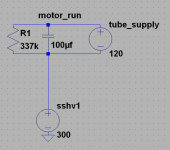
Stacking supply from SSHV1
Hi,
I am wondering if there is some reason I would not be able to stack a tube rectified supply with a SSHV1. The SSHV is working as expected when it is used independently. When testing the tubed supply independently, it also operates as expected. However, when the tubed supply is stacked on top of the SSHV, I am left with what seems to be some kind of short. I have not checked the current in this condition, but the output voltage measures as 0v. The return of the tubed supply is simply connected to the positive output of the SSHV. The SSHV supply return is connected to signal and earth ground, while the tubed supply's return is only connected to the positive terminal of the SSHV. The SSHV output does not have a load on its output, and the tubed supply output is not regulated, its only load is bleeder resistors. I should also note that the raw supply for the SSHV is SS rectified by a UF4007 FWB, and (small first C)LC filter. I'm sure that I am missing something and that someone can shed some light on this. I have stacked supplies before in prototypes, but never with an SSHV and tubed supply like this.
Regards,
-Michael Woods
Attachments
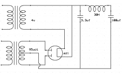
Surely you need to stack two AC windings on the CT main winding.
Add a 4Vac winding on to one side of the 95Vac CT and add a 4Vac winding to the other side of the 95Vac CT. Now you have 103Vac CT to send to the rectifier.
I cannot see how your 4Vac added after the or through the rectifier output can work.
Add a 4Vac winding on to one side of the 95Vac CT and add a 4Vac winding to the other side of the 95Vac CT. Now you have 103Vac CT to send to the rectifier.
I cannot see how your 4Vac added after the or through the rectifier output can work.
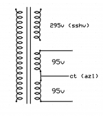
I might need to move this post, because I realized it's really in the wrong thread! Anyway, the 4v supply is just the filament winding for the az1. The 95vac supply ends up being the 120vdc, which I want to stack off of the 295vac winding supply that is 350vdc raw and 300vdc after regulation.
-MW
-MW
Hi !
Quick question.
I recently received a set of SSHV2 boards. I'm planning on using them for a phono preamp. It uses 4x C3g tubes, each biased at 18ma.
The documents state the max current is 100ma. I'm assuming this is max CCS current ?
If so, given my load is 72ma, if my CCS is set at 100mA, that leaves with 28mA of shunt current. Is that enough for the board to perform ?
I'm not planning to drop too many volts over the regulator (each tube is loaded by a CCS, so I'll let those drop the voltage). Votlage in will be about 260V.
- Home
- Amplifiers
- Power Supplies
- Simplistic mosFET HV Shunt Regs