In some cases the use of TMC produces a sharp increase in loop gain in the middle of the audio band. This peak can be eliminated by the inclusion of a 10n cap in series with R20.
Gotcha, thanks! but to my understanding that peaking midband is a problem with TPC, TMC doesn't have that problem.
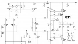
Thanks BesPav, that's very elegant indeed, thanks for the suggestion. See attached updated schematic.
Aaargh, i can't found updates in schematic!
I would love to hear what suggestions you have for this! 😀
He-he! I'ld put an opamp in front of the schematic.
First of - to obtain as much gain as we could cope. Discrete fails because too huge size, capacitance and unpredictable fingerprints at the high-impedance point, so compromised feedback depth.
I'ld take your OPS and put it somewhere here:
Opamp + Common base
This will add something like 40-50 dB feedback depth at 20kHz with conservative unity gain freq in range of ones of MHz or even more if you allow your amp to be High-frequency transmitter in the range of tens of MHz.
Also i'ld try famous AD844 as inout stage and pick it's output signal from their supply pins. Again, up to 50-60 dB feedback depth at 20 kHz.
Am i need to draw?
BTW, your ExtremA amp was a beauty! Hot beauty!
How do you control output offset without using a dc blocking cap in the NFB circuit ?
R7+R8 will be a trimpot, so I can set offset after the amplifier has warmed up, I'm seeing uVs in the simulator, if that turns out to be too optimistic and I see large (10s of mV) in practice I might opt for a DC servo.
If you haven't done so, you may want to model temperature and supply voltage changes. They can have significant impact on DC offset in the absence of a blocking cap.
I've used an approach like this for temperature:
These allow you to specify and vary the global temperature of the simulation:
PHP:
.param T=35
.step param t list 20 30 40
These allow you to specify if the simulation if from a cold or hot state:
PHP:
.param Thot=1
.step param Thot list 0 1
Finally each device in the simulation is modeled for it's temperature rise. I do this for all active devices. You'll need to calculate the expected rise in each device:
PHP:
 .param Tips = {{T} + (10 * {Thot})}
 .param Tvas = {{T} + (25 * {Thot})}
 .param Tdvr = {{T} + (5 * {Thot})}
 .param Tops = {{T} + (25 * {Thot})}
And finally, here's an example of how an input device is specified:
PHP:
BC550C temp={Tips}In my simulations, I've found that the DC offset can vary considerably with temperate if blocking caps aren't used.
This type of analysis can also be used to assess how stable the output stage bias is with respect to temperature.
Of course, this all assumes that temperature simulation in LTSpice accurately models reality.
Aaargh, i can't found updates in schematic!
Please see attached, is this what you meant with connecting Q6 as a diode?
He-he! I'ld put an opamp in front of the schematic.
Ah yes, that was one thing I explored as well, if I reduce the gain of my amplifier to for example 5x and put an instrumentation amplifier in front, for example a LM4562 or a OPA1656 with a gain of 4x, then I get much lower THD, well below -120dB/100W/8R/20kHz actually.
I could also take it a step further and make a composite amplifier, and have a feedback loop around the entire amplifier using an opamp, this will push THD even lower. However I first want to see how far I can push this simple discrete design.
BTW, your ExtremA amp was a beauty! Hot beauty!
Thanks, but I can't take all the credit though, most of the design work was done by Bruno Putzeys, I optimized the design in the simulator and built and evaluated several prototypes.
Attachments
Thank you so much for this information.
My builds will be simpler without the diodes.
Be careful though, I've only verified this for the ECW20x20 double-die Exicon lateral MOSFETs, I don't know if the same applies to the single-die versions you appear to be using?
If you haven't done so, you may want to model temperature and supply voltage changes. They can have significant impact on DC offset in the absence of a blocking cap.
<snip>long, interesting reply</snip>
Most excellent, thanks! I've thusfar only modelled the Tjunction temperature of the lateral MOSFETs (you'll notice the Spice directives in the schematic), but it indeed makes sense to look at the DC offset behavior of the entire amplifier.
Please see attached, is this what you meant with connecting Q6 as a diode?
Draw faster than write, so i've attached.
I could also take it a step further and make a composite amplifier, and have a feedback loop around the entire amplifier using an opamp, this will push THD even lower. However I first want to see how far I can push this simple discrete design.
The main disadvantage of discrete design with high gain is repeatability.
High gain anyway asks for conditionnaly stable compensation of, say, 2-3 or even higher orders.
But using simulator you can't predict PCB leaks and cleaning quality of each user, so there anyway will be unstable builds.
So, being optimistical about following builder abilities and understanding, i'ld not try to pick too much gain from discrete design. At least one high-impedance (high-gain) point are better to keep inside the crystal.
Attachments

Last edited:
Draw faster than write, so i've attached.
Ah yes, of course, thanks!
The main disadvantage of discrete design with high gain is repeatability.
High gain anyway asks for conditionnaly stable compensation of, say, 2-3 or even higher orders.
I have 20+ years of PCB layout experience, including high frequency RF (>5GHz) so I'm not worried about the layout, and quite frankly I have a electronic solution to deal with inductive rail coupling and distortion related to it, this was first proposed by Edmond Stuart and Dimitri Danyuk. Please find the working principle attached.
Pickup off points A1, A2, B1 and B2 are routed to 4 resistors, connected to the junction between the two TMC capacitors. So what does this accomplish? This is for balancing mutual inductive influence from powerrail loops by slightly varying the values for these resistors so inductive coupling of the PCB can be minimized.
Attachments
just check the Bode diagram and look at the Group Delay to say that the parameters of this amplifier will be at their best
Attachments
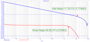
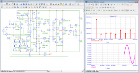
Thanks petr_2009 for taking the effort to simulate the design, much appreciated! Could you perhaps illustrate what these graphs mean? The loop gain/phase and margin plots are self explanatory, but the others have me scratching my head a little, what am I looking for in those?
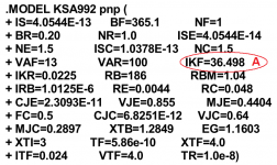
strange parameter
These are models from the Fairchild website, as I’m using exactly these transistors. Not sure what that parameter means exactly.
The loop gain/phase and margin plots are self explanatory, but the others have me scratching my head a little, what am I looking for in those?
I agree. I found the charts confusing. It's not clear to me what they represent.
collector current at which the base current transfer ratio begins to decline (high-current roll-off corner)These are models from the Fairchild website, as I’m using exactly these transistors. Not sure what that parameter means exactly.
Could you perhaps illustrate what these graphs mean?
I found the charts confusing. It's not clear to me what they represent.
Folks, keep your keyboards bewared about trolls.
try these models
.MODEL 2SC1845E_kq npn IS=1.075431E-13 BF=600.7 NF=1 BR=13.565 NR=1 ISE=1.98107E-13 NE=2 ISC=1.8378E-11 NC=1.5 VAF=200 VAR=20.6691 IKF=55m Nk=0.66 IKR=0.0190546 RB=157 RBM=12.092 IRB=1.258925E-6 RE=1.5 RC=1 CJE=18p VJE=0.7300286 MJE=0.3619943 FC=0.5 CJC=4.525739E-12 VJC=0.5 MJC=0.3659045 XTB=1.7281 EG=1.1809 XTI=3 Tf=420p Itf=20m Xtf=1 Rco=250 gamma=2u Vo=500 Vceo=120 Icrating=50m mfg=NEC
.model KSC1845F_kq ako:2SC1845E_kq NPN Vceo=120 Icrating=50m mfg=Fairchild Bf=355 Ikf=300m Vaf=400 Ise=1000f Ibc=600f Rco=150 Gamma=10u Vo=9 Isc=22f
.MODEL 2SA992F_kq pnp (IS=5.7544E-14 BF=348.1 NF=1 BR=3.62 NR=0.95 ISE=5.7544E-15 NE=1.5 ISC=1.8378E-14 NC=1 VAF=50 VAR=16.68 IKF=0.298 IKR=0.0525 RB=140 RBM=16.084 IRB=1.4125E-3 RE=0.3 RC=100m CJE=13p VJE=0.855 MJE=0.4104 FC=0.5 CJC=8.9251E-12 VJC=0.5 MJC=0.3497 CJS=0 VJS=0.8 MJS=0.33 XTB=1.2849 EG=1.1603 XTI=3 XCJC=0.3062 Tf=420p Itf=5 Xtf=.5 Vceo=120 Icrating=50m mfg=NEC Rco=100 gamma=200n Vo=500)
.model KSA992F_kq ako:2SA992F_kq PNP Vceo=120 Icrating=50m mfg=Fairchild Bf=404 Vaf=110 Ikf=150m Ise=15f Isc=0.0010f Rco=70 Rc=0 Gamma=1500n Vo=100 Ibc=45f Is=75f
BesPav - you yourself are a troll if you don't understand chartsFolks, keep your keyboards bewared about trolls.
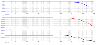
1. Ssassen_Rout graph - filmed by applying a signal to the amplifier output through an 8 ohm resistance. This is the common way to measure the output impedance of an amplifier. Output impedance is calculated using the formula: Rout = RL * Vout / (Vin-Vout)
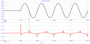
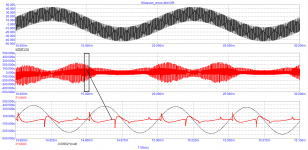
2. 2. Switching distortion is measured using a specially designed filter for this purpose. A complex signal of 100 Hz and 20 kHz is fed to the amplifier input. The filter cuts out these signals and at the output of the 50 Ohm matched filter we get the distortion products as shown in the Ssassen_cross-dist graph.
3. 3. Graph Ssassen_20kHz-spectr - the result of measuring the spectrum in the fourth period.
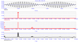
I hope that the IMD measurement graph does not need comments
- Home
- Amplifiers
- Solid State
- Simplicity and elegance, feedback wanted!