THanks Lazy. I will actually be running them at 26V rails, as this is all that i can muster without buying new trafo. I may play with bias a little on final product.
BC550C/BC560C (2SA970/2SC2240) are suitable for both stages if the rail supply voltages are +/-35V and cascode collector current is 2 to 5mA, so to keep them safe from Vce-max and power dissipation point of view.
If supply voltages are higher I recommend BF471/BF472, 2SA1478/2SC3788 or similar TO-126 case high bandwidth transistors. 😉
Please note that the pin config of 2SA970/2SC2240 is different to BC550C/560C you cannot drop one in place of the other.
Nico
Lazy....That bigbt....is that one you have built yourself...or..??
think that a version with the lateral fets Sk216/SJ79.. would improve thing further....lower COB and negative tempco, so you can take away the VBE transistor...
think that a version with the lateral fets Sk216/SJ79.. would improve thing further....lower COB and negative tempco, so you can take away the VBE transistor...
Please note that the pin config of 2SA970/2SC2240 is different to BC550C/560C you cannot drop one in place of the other.
The 2SA and 2SC parts look like the best, in terms of voltage and Hfe linearity over a wider range. Looks like mass quantities available on e-bay. So much so, that one wonders if they are genuine (don't need to be Toshiba mnf, if they have the same performance). Anyone with experience?
Sheldon
Please note that the pin config of 2SA970/2SC2240 is different to BC550C/560C you cannot drop one in place of the other.
Nico
Thanks Nico, I already mentioned that to Alex at the begining of my post #434. 🙂
Sorry LC, I was actually voicing a comment to those who may build and insert BC550/560 into Alex's board without realizing this. No criticism meant.
Nico
Nico
Lazy....That bigbt....is that one you have built yourself...or..??
think that a version with the lateral fets Sk216/SJ79.. would improve thing further....lower COB and negative tempco, so you can take away the VBE transistor...
Yes that's the one I pushed hard 😀
Mhmm you think an all mosfet output, drivers and output's? Nice one too. 🙂
Sorry LC, I was actually voicing a comment to those who may build and insert BC550/560 into Alex's board without realizing this. No criticism meant.
Nico
Nico you are my friend, no hard feelings at all. 😉
We are together in this project and stating out such detail is good for everyone as potential builders. We all have to be precise at details. 😉
LC..
I think a combo device like yours... but with lateral fets instead of the verticals...then the device will balance itself thermaly...and the lower cob of the laterals will increase performance as well
I think a combo device like yours... but with lateral fets instead of the verticals...then the device will balance itself thermaly...and the lower cob of the laterals will increase performance as well
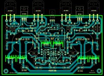
Ahaa a little more spacious PCB ... gooood. 😎
Very nice Alex, I am sure tomorrow's version will be PCB art in best possible way. Than we'll make fine tuning and it will be just perfect.
Very nice Alex, I am sure tomorrow's version will be PCB art in best possible way. Than we'll make fine tuning and it will be just perfect.
LC,
How about a diamond buffer output stage? Have you considered this, said to sound very good.
Cheers,
Hugh
How about a diamond buffer output stage? Have you considered this, said to sound very good.
Cheers,
Hugh
Nano Diamond Transistors, Operate in Vacuum - Better Than Tubes?
" DIAMOND TRANSISTORS "
From the txt . . .
here: http://news.vanderbilt.edu/2011/08/nanodiamond/
This transmission efficiency is also one reason why the new devices can run on very small amounts of electrical current. Another is that diamond is the best electron emitter in the world so it doesn’t take much energy to produce strong electron beams. “We think we can make devices that use one tenth the power of the most efficient silicon devices,” said Davidson.
The design is also largely immune to radiation damage. Radiation disrupts the operation of transistors by inducing unwanted charge in the silicon, causing an effect like tripping the circuit breaker in your home. In the nanodiamond device, on the other hand, the electrons flow through vacuum so there is nothing for energetic particles to disrupt. If the particles strike the nanodiamond anode or cathode, the impact is limited to a small fluctuation in the electron flow, not complete disruption, as is the case with silicon devices.
Scanning electron microscope image of a nanodiamond transistor. (Davidson Lab)
“When I read about the problems at the Fukushima power plant after the Japanese tsunami, I realized that nanodiamond circuits would be perfect for failsafe circuitry in nuclear reactors,” Davidson said. “It wouldn’t be affected by high radiation levels or the high temperatures created by the explosions.”
Nanodiamond devices can be manufactured by processes that the semiconductor industry currently uses. The one exception is the requirement to operate in vacuum, which would require some modification in the packaging process. Currently, semiconductor chips are sealed in packages filled with an inert gas like argon or simply encapsulated in plastic, protecting them from chemical degradation. Davidson and his colleagues have investigated the packaging process and have found that the metallic seals used in military-grade circuitry are strong enough to hold an adequate vacuum for centuries.
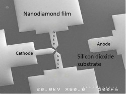
Better Days also for Audio are coming ?
Watch webcast of Davidson talking about the first nanodiamond vacuum emitter device logic circuits.
Cheers
A.
" DIAMOND TRANSISTORS "
From the txt . . .
here: http://news.vanderbilt.edu/2011/08/nanodiamond/
This transmission efficiency is also one reason why the new devices can run on very small amounts of electrical current. Another is that diamond is the best electron emitter in the world so it doesn’t take much energy to produce strong electron beams. “We think we can make devices that use one tenth the power of the most efficient silicon devices,” said Davidson.
The design is also largely immune to radiation damage. Radiation disrupts the operation of transistors by inducing unwanted charge in the silicon, causing an effect like tripping the circuit breaker in your home. In the nanodiamond device, on the other hand, the electrons flow through vacuum so there is nothing for energetic particles to disrupt. If the particles strike the nanodiamond anode or cathode, the impact is limited to a small fluctuation in the electron flow, not complete disruption, as is the case with silicon devices.
Scanning electron microscope image of a nanodiamond transistor. (Davidson Lab)
“When I read about the problems at the Fukushima power plant after the Japanese tsunami, I realized that nanodiamond circuits would be perfect for failsafe circuitry in nuclear reactors,” Davidson said. “It wouldn’t be affected by high radiation levels or the high temperatures created by the explosions.”
Nanodiamond devices can be manufactured by processes that the semiconductor industry currently uses. The one exception is the requirement to operate in vacuum, which would require some modification in the packaging process. Currently, semiconductor chips are sealed in packages filled with an inert gas like argon or simply encapsulated in plastic, protecting them from chemical degradation. Davidson and his colleagues have investigated the packaging process and have found that the metallic seals used in military-grade circuitry are strong enough to hold an adequate vacuum for centuries.
Better Days also for Audio are coming ?
Watch webcast of Davidson talking about the first nanodiamond vacuum emitter device logic circuits.
Cheers
A.
Ah, not quite what I meant, but interesting nonetheless......
I think these devices would be very suitable for hard rock, I really do.
Hugh
I think these devices would be very suitable for hard rock, I really do.
Hugh
Hugh,
They will absolutely shine in what You have in minds, but they must of course also to invent a PNP one.. than will be possible . . .
Music ... for Rock no doubt, and for nice Instrumental, Classical, Vocal, Jazz and for some heavy Dub Reggae too . . 🙂
Cheers
A.
They will absolutely shine in what You have in minds, but they must of course also to invent a PNP one.. than will be possible . . .
Music ... for Rock no doubt, and for nice Instrumental, Classical, Vocal, Jazz and for some heavy Dub Reggae too . . 🙂
Cheers
A.
LC,
How about a diamond buffer output stage? Have you considered this, said to sound very good.
Cheers,
Hugh
Hugh, you've just found yourself your SSA.

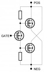
LC..
I think a combo device like yours... but with lateral fets instead of the verticals...then the device will balance itself thermaly...and the lower cob of the laterals will increase performance as well
You have in mind something like this? 🙄
Attachments
See Post!
Hi Alex mm (POP Alexandru) !
Please refer to this topic:"80W hybrid audio amplifier"!?😱
thanks
Hi Alex mm (POP Alexandru) !
Please refer to this topic:"80W hybrid audio amplifier"!?😱
thanks
Last edited:
LC....
I was thinking your basic circuit, but with lateral fets (2SK216/2SJ79 instead of the IRF 9610/610.. the laterals have only two third's of the Ciss capacitance...and also negative tempco...So I believe you can take away the VBE and instead use the simpler resistor biasing
I was thinking your basic circuit, but with lateral fets (2SK216/2SJ79 instead of the IRF 9610/610.. the laterals have only two third's of the Ciss capacitance...and also negative tempco...So I believe you can take away the VBE and instead use the simpler resistor biasing
- Status
- Not open for further replies.
- Home
- Amplifiers
- Solid State
- Simple Symetrical Amplifier