Very well Bigun, nice incarnation of SSA. 😎
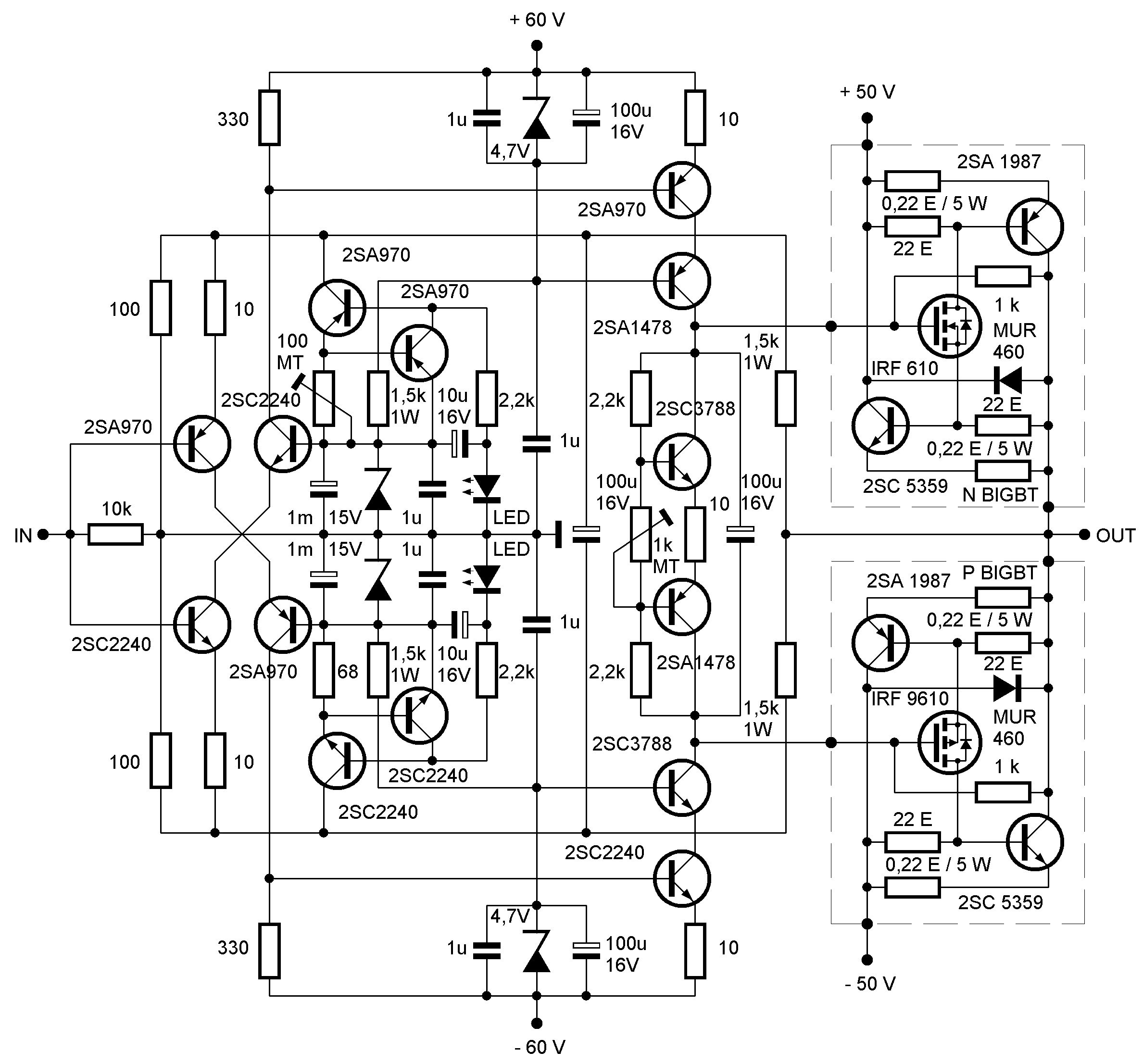
OLG adjustment:
- R2 ratio to R20
- R7 ratio to R19
- R14 ratio to R16
- R15 ratio to R21
- omit R3, R8 you don't need these two at +/-36V rails
CLG adjustment:
- R5 ratio to R1 +1
- R10 ratio to R6 + 1
- both loops symmetrically adjusted
Please feel freely to experiment further. 😉
OLG adjustment:
- R2 ratio to R20
- R7 ratio to R19
- R14 ratio to R16
- R15 ratio to R21
- omit R3, R8 you don't need these two at +/-36V rails
CLG adjustment:
- R5 ratio to R1 +1
- R10 ratio to R6 + 1
- both loops symmetrically adjusted
Please feel freely to experiment further. 😉
Hi All,
I think there are three "tested" schematics here, the L-MOSFET, Michael's (MiiB) BJT version and Andrej's IGBT version.
If I may suggest that Alex would could start a thread where his PCB layout and the associated "tried" schematics are posted for those who want to build and try this superb design for themselves without having to search 400+ posts, but keep that thread totally uncluttered of comments other than PCB layout comments.
Why I am suggesting Alex if he has the time is that he is the only one that has a schematic and BOM that matches up with a PCB on his computer.
Discussions and new ideas remain here on this thread. Any comments on this suggestion?
Regards
Nico
Very good idea Nico. 😉
I would only suggest that all incarnations-versions starts with the SSA name to know the general topic and than the name of the specific version. That would be polite and reasonable to DIY members interested to built and to search among the SSA threads. 🙄
OK, can be also different of course. 🙂
Thanks Andrej. How about it Alex, are you prepared to do this. Of course there is no hurry.
It will aid a lot of members that are late joiners or just want to build a great amp without tediously studying this thread to pull the pieces together.
It will aid a lot of members that are late joiners or just want to build a great amp without tediously studying this thread to pull the pieces together.
Hi all!
I can not wait to get to a "happy end", ... good power amplifier with UCC=+ /-36V and output complementary pair 2SC5200/2SA1943!
Then I will build it, let's go ahead and,.. ...!
Regards
I can not wait to get to a "happy end", ... good power amplifier with UCC=+ /-36V and output complementary pair 2SC5200/2SA1943!
Then I will build it, let's go ahead and,.. ...!
Regards
That's what happens when we have a thread with 100 schematics and neither of them has a clear, distinctive name... 😱
The best we can do now is to refer to them by post number.
Yes Juma, it is getting difficult to keep track of good , better, best ..🙂
LC, Nico, Alex,
May i suggest a board incorporating the original SSA, the modded SSA as now being used by LC /Nico and the bigger more powerful version as suggested with 8 outputs/ch. This way with one board one could build all or any version of the SSA, similar to what was done by Cvilliers for the F5 ..
regards,
Hi Nico,
Did you change the C12 & C13 from 12pF to 3.3pF?
You also said that you would implement some of the MiiB's changes, can you please post your latest schematics?
Best regards, Stanley
Yes I have changed to 3,3pF from 12pF which rolled off to quickly. I have approximately 80 degrees phase margin which is ample. Does it sound different - Absolutely not. It may irritate some bats.
Yes Juma, it is getting difficult to keep track of good , better, best ..🙂
LC, Nico, Alex,
May i suggest a board incorporating the original SSA, the modded SSA as now being used by LC /Nico and the bigger more powerful version as suggested with 8 outputs/ch. This way with one board one could build all or any version of the SSA, similar to what was done by Cvilliers for the F5 ..
regards,
Might be a mind bender for Alex, but I think he is a clever boy.

There is a special artistry involved when laying out a decent looking as well as working PCB - some has it most just cannot, You have mastered this art Alex. I start a PCB the same time as you taking me hours then it looks like puke. You do it in a lot less time and it turns out a masterpiece.
There is a special artistry involved when laying out a decent looking as well as working PCB - some has it most just cannot, You have mastered this art Alex. I start a PCB the same time as you taking me hours then it looks like puke. You do it in a lot less time and it turns out a masterpiece.
I hope one day to be able to lay out stable, good looking pcbs for solid state amps, even half as good as alex mm.
Right now I can only do power supplies and such.
Maybe I better get learning if I want my special size boards for this amplifier. Or, I will have to find somebody and pay them.
But then that still leaves the amp. I need a two pair BJT version to run off of +-~50VDC... Guess I will have to get sketching and see if I can't come up with it myself. And not screw it up.
As for suggestions for boards, I would go with what somebody said a little bit ago -- maybe have a seperate board for input circuitry and seperate interchangeable boards for output stage. This would make things more universal, and people could just as well switch out output stages to see the result without redesigning a whole new PCB for it all.
Yes I have changed to 3,3pF from 12pF which rolled off to quickly. I have approximately 80 degrees phase margin which is ample.
Hi Nico,
Thanks for the answer.
I also agree that AlexMM is the master of PCB layout, he consistently outperform himself. I will fiddle with his single-LFET version a tiny bit to fit an existing heatsink & bigger filter capacitors.
Cheers, Stanley
I second that, Nico. Alex is the best pcb artist I've seen on DIYaudio, and he's fast, too.
I spend tens of hours on mine, and it's always difficult to get that artistic look, which necessary or not, I'm driven to achieve. I suspect it's like juggling, you can either do it or you can't.
Cheers,
Hugh
PS: Here are six NAKSA 100 modules, to give some idea of how mine look.
I spend tens of hours on mine, and it's always difficult to get that artistic look, which necessary or not, I'm driven to achieve. I suspect it's like juggling, you can either do it or you can't.
Cheers,
Hugh
PS: Here are six NAKSA 100 modules, to give some idea of how mine look.
Attachments

I just started playing with Pcb software and quickly realized the time and effort it would take to master, much less do quickly. Alex is gifted.
Yes I agree, SSA could be a very good RF transmitter amp up to 10MHz bandpass.
On mine PCB there will also be a space for these two caps, to have exact -3dB bandwidth limit. Also I will limit the input signal bandwidth with low-pass filter set to -3dB at 1MHz. 😀
So the input CF diff-amp and unique feedback loop determine the sound character in general. 😎
This is very important info Nico, thanks, cause I only experimented with BIGBT's and for my home amp I have intent to do a little more sophisticated version, hopefully the sound will stay the same. 🙄
Yes, IGBT and MOSFET output versions are the simplest.
Regards, Andrej 😉

This schematic, which shows BC550/560 in both bjt stages, should work fine with mosfet output, correct?
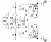
SSA BIGBT Basic
Dear Alex here are the remarks about SSA BIGBT Basic PCB, can you please make all these corrections:
- BC550C, BC560C have different pin layout (base connection pin in the middle)
- left feedback 100 ohm resistor is unconnected, connect it to the GND
- change two 470uF/16V elco to 1000uF/16V
- on the left side of the input connector place a 10 ohm GND lift resistor (opposite side to 10k resistor)
- 1k/2W resistor should be connected to the rails at FUSE output
- in series with each 1k/2W resistor please connect green LED to indicate power
- please put MUR160 (smaller) instead of MUR460
- Vbe multiplier transistor should be BD139 instead of BC550C, screw mounting to heatsink
- please align output transistors symmetricaly from the left/right PCB edge
- please give +1mm more space between outputs/drivers (too close to each other)
- trimer 1k should be near to BD139, you have than only two jumpers wires
- please put (sch below) 10 ohm emitter resistor to Vbe multiplier
- rearrange positions of 1k/2W resistor, 1uF, 10nF, to put 10000uF/63V on PCB
- place one more GND connection (SPK-) in between two existing (three in the line)
- place only one OUT pin connector in the middle
- 1k feedback resistors should be connected at exact OUT pin (not 2 cm away)
- 1k from each gate of IRF to emitter of the output BJT are missing
- please put two 15V/0,5W zener diodes in series (chatodes towards each other) from gate to source of each IRF (overvoltage gate protection)
- heatsink from each power diode MUR860, should have holder solder pin, like at BF's
- the name of the PCB: SSA BIGBT Basic
- the schematic is by Lazy Cat 😉
......and now rev 1.5 for BIGBT variant ......🙂 please check PCB for errors , not tested .
Alex.
Dear Alex here are the remarks about SSA BIGBT Basic PCB, can you please make all these corrections:
- BC550C, BC560C have different pin layout (base connection pin in the middle)
- left feedback 100 ohm resistor is unconnected, connect it to the GND
- change two 470uF/16V elco to 1000uF/16V
- on the left side of the input connector place a 10 ohm GND lift resistor (opposite side to 10k resistor)
- 1k/2W resistor should be connected to the rails at FUSE output
- in series with each 1k/2W resistor please connect green LED to indicate power
- please put MUR160 (smaller) instead of MUR460
- Vbe multiplier transistor should be BD139 instead of BC550C, screw mounting to heatsink
- please align output transistors symmetricaly from the left/right PCB edge
- please give +1mm more space between outputs/drivers (too close to each other)
- trimer 1k should be near to BD139, you have than only two jumpers wires
- please put (sch below) 10 ohm emitter resistor to Vbe multiplier
- rearrange positions of 1k/2W resistor, 1uF, 10nF, to put 10000uF/63V on PCB
- place one more GND connection (SPK-) in between two existing (three in the line)
- place only one OUT pin connector in the middle
- 1k feedback resistors should be connected at exact OUT pin (not 2 cm away)
- 1k from each gate of IRF to emitter of the output BJT are missing
- please put two 15V/0,5W zener diodes in series (chatodes towards each other) from gate to source of each IRF (overvoltage gate protection)
- heatsink from each power diode MUR860, should have holder solder pin, like at BF's
- the name of the PCB: SSA BIGBT Basic
- the schematic is by Lazy Cat 😉
Attachments
Last edited:
According to my current needs and personal taste I will start to make something like this. 😎
http://www.diyaudio.com/forums/atta...591-simple-symetrical-amplifier-ssa-bigbt.jpg
Why two decoupling caps for the input voltage shunt reg? Why not just put the 1m cap in place of the 16u cap to the LED?
Sheldon
Hi Sheldon,
10uF/16V elcos are decoupling current source/sink generators (sense BJT) not +/-15V rails 😉
10uF/16V elcos are decoupling current source/sink generators (sense BJT) not +/-15V rails 😉
Hi Sheldon,
10uF/16V elcos are decoupling current source/sink generators (sense BJT) not +/-15V rails 😉
As a practical matter, is there much difference? That node (LED) should present a very low impedance to common, and LED's are very quiet. Just curious.
Sheldon
Last edited:
I know but this amp has several MHz power bandwidth and replacing current supply resistor with current source/sink is critical. All unwanted AC, RF, ripple, ... must be rejected from sense BJT's collector to prevent any kind of oscillations in CSS generators. 😉
This schematic, which shows BC550/560 in both bjt stages, should work fine with mosfet output, correct?
BC550C/BC560C (2SA970/2SC2240) are suitable for both stages if the rail supply voltages are +/-35V and cascode collector current is 2 to 5mA, so to keep them safe from Vce-max and power dissipation point of view.
If supply voltages are higher I recommend BF471/BF472, 2SA1478/2SC3788 or similar TO-126 case high bandwidth transistors. 😉
- Status
- Not open for further replies.
- Home
- Amplifiers
- Solid State
- Simple Symetrical Amplifier