Would you be open to sending the code for the project?
SMathews
SMathews
Hi xx3stksm!
As they say, a picture is worth a thousand words, I send you complete list of coeffs and modulator vhdl code.
The code is without reset and dither for clarify.
You can easily check how it is done.
Olek
No problem, you just need to find someone to take care of it.
Thanks Olek. Are you or Pjotr able to include a 'pick and place' file with the Gerbers?
Could you clarify CSD arithmetic in detail or reference paper?
https://shareok.org/bitstream/handle/11244/1254/3283840.PDF?sequence=1
This is a gerber files with attached 'pick and place' files mnt and mnb.
Thank you, I'll make some enquiries to see if a small group buy for assembled boards will be viable.
nautibuoy,
If Olek & Pjotr are OK with this, I'd be happy to build a small batch of boards (test / program them) if you dont find other options (currently located in mainland Europe)...
If Olek & Pjotr are OK with this, I'd be happy to build a small batch of boards (test / program them) if you dont find other options (currently located in mainland Europe)...
Last edited:

As far as I know, everyone determines the dithering level for a single-bit sigma-delta experimentally, because dither theory only applies when you have more quantization levels available.
good to know...thx
Would you be open to sending the code for the project?
SMathews
unfortunately no, I have other plans .....
If Olek & Pjotr are OK with this, I'd be happy to build a small batch of boards (test / program them) if you dont find other options (currently located in mainland Europe)...
of course ok 🙂
nautibuoy,
If Olek & Pjotr are OK with this, I'd be happy to build a small batch of boards (test / program them) if you dont find other options (currently located in mainland Europe)...
Thanks John, I'll PM you.
Ray
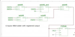
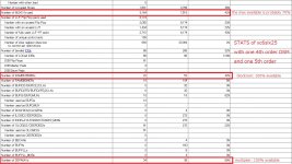
olo111 and Markw4, Thanks for your information. I have almost understood what CSD means. Multiplierless solution is fantastic, indeed.🙂 But I think you need to tweak CSD for a specific FPGA architecture because the adder also has the limitation; available numbers and speed. As you know, CRFB requires six inputs adder if you include local FBs(g0,g1,g2). Three stages adder(pic.1) is probably max due to propagation delay. It occupies many adders. The very trouble that forces me to fail the routing is not the lack of multiplier but adder, which is invisible even in ISE circumstance(pic2). My strategy is usually full usage of block ram and multiplier(100% guaranteed) and as little usage adder as possible. Xc6slx25 can implement up to two 6th order DSM in 160OSR. Of course, I guess you have a CSD-based strategy. 😉
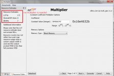
A similar technique like CSD is a constant coefficient multiplier, which replaces a multiplier with block ram. Pic3 is multiplier less calculation of g1(0x16e4632b) for local FB. The calculation of a0,a1,,,, and a6 doesn't need a multiplier, too. The total number you need to calculate DSM is six 18x18 multipliers, acceptable even with a small FPGA(xc6slx25). That's my strategy, and you have another one. It's wonderful everyone has their way. 🙂🙂
Attachments
Last edited:
Where're flash file for upload to XC6SLX9 IC. Tks u ��Hi,
As olo said, I put boom and gerber files.
PCB it is 4 layers and dimension 69x40mm.
Where're flash file for upload to XC6SLX9 IC. Tks u ��
In the first post.
It's "top.bit" file. Tks u
This board are accept any I2S format 16/20/24/32-bit length, and maximum of sampel rate are 192Khz !?
This board are accept any I2S format 16/20/24/32-bit length, and maximum of sampel rate are 192Khz !?
Last edited:
As Olek wrote in the first post, the modulator was written for sample rates from 44.1 to 192kHz.
Not tested above 192kHz.
It accepts a length of 16-32 bits, but there are 24 bits inside.
DSD is passed thru unchanged.
Not tested above 192kHz.
It accepts a length of 16-32 bits, but there are 24 bits inside.
DSD is passed thru unchanged.
Can we use the Development Kit as attached !? Mojo V3 FPGA Development Board Module Spartan 6 XC6SLX9 FPGA for Arduino US|Integrated Circuits| - AliExpress
As I see you are using Eagle PCB, can you share the schematic, map, pinout of this project !?
Thank you again for the community.
As I see you are using Eagle PCB, can you share the schematic, map, pinout of this project !?
Thank you again for the community.
Attachments

Last edited:
Please forgive me for the inconvenient questions. I have not found the .sch and .brd files in the files you shared in pcm2dsd_gerber.zip and pcm2dsd_boom.zip
Can you share the schematic as a *.pdf file !?
I want quick try it on "https://a.aliexpress.com/_mtWaXJ5" available in my country and I need schematic or pinout mapping on your board.
Can you share the schematic as a *.pdf file !?
I want quick try it on "https://a.aliexpress.com/_mtWaXJ5" available in my country and I need schematic or pinout mapping on your board.
This a board is good for prototypes, for the final product many details are important (PCB too)...
We've shared gerbers files to do it as best as possible...
We've shared gerbers files to do it as best as possible...
Thank again.This a board is good for prototypes, for the final product many details are important (PCB too)...
We've shared gerbers files to do it as best as possible...
I will use the your gerber for try this.
It's easily for debug and your support.
- Home
- Source & Line
- Digital Line Level
- Simple DSD modulator for DSC2