No originality claimed here.
John, but I was saying that the current source lowered the noise. i.e. the noise was higher with the resistor load.
I was just kidding about .1nV/rtHz. Sometimes I find it a bit silly how some take themselves so seriously here. Some of us are just having a bit of hobby fun. There's enough discipline and rigour in other parts of my life.
Then, what is the self noise of the power supply? That might get through the resistor.
Then you would have traded the noise addition of the current source and against the increased power supply rejection. Might be some tradeoff there.
You should see what I have to go through to make a low noise power supply.
Then you would have traded the noise addition of the current source and against the increased power supply rejection. Might be some tradeoff there.
You should see what I have to go through to make a low noise power supply.
This is a little bit clearer -- you can grab a beer between averaging the analyzer -- the SSM2019 has fewer issues with 1/f noise than the Colin Low Noise amp. (The case in which this SSM2019 is housed appears a little problematic.) I used the AP "equiripple" window, and averaged 256X.
The Colin amp, an LSK389 followed by an AD797 yields 1.9nV @10kHz, but 7.0nV @100 Hz. The SSM2019 @60dB is 3.1nV +/- 0.1nV down to 20Hz. The SSM2019 is least noisy at +60dB.
The thing which I will have to do is get your final design, put one together, and compare the lot. I think that the analyzer in analog bandpass mode may be better for low noise signals, but in digital mode you can see the problems in the low end of the range.
Nice to see these results posted.
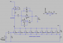
Jack, the schematic for what I built now is above, except the load resistor is replaced with a couple of paralleled jfets. I would suggest you implement a properly engineered circuit like syn08's or Samuel's design. If you're really curious about the contraption that I got here I'll give you the details needed to build it. At least you don't need to be converted to cookie tins 🙂
Then, what is the self noise of the power supply? That might get through the resistor.
Then you would have traded the noise addition of the current source and against the increased power supply rejection. Might be some tradeoff there.
You should see what I have to go through to make a low noise power supply.
Indeed, I left this part out of my previous message, I was curious who'd catch it.
The psu is lead acid batteries, with local decoupling capacitors of various values. The batteries are inside the tin can, which has the lid on when I run the measurement. When the lid is off the noise is quite a bit higher. When the tin can is physically closer to the the analyzer the noise increases again. I know, this shows that the tin can isn't doing a terribly good job at keeping out EMI.
Edit: and I have paid a lot of attention to your stories about the power supply for your preamp. With the three stages, etc.
I think I have some NiCr wire at work. Perhaps I'll try to make a load resistor with that and measure again. Time to call it a night now.
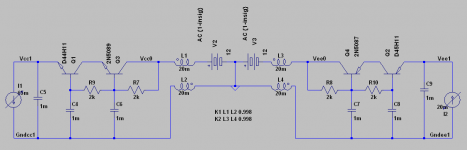
These are the experiments I've tried. First, the attached circuit measures for me around 0.43nV/rtHz at 1kHz.
1) to rule out that the noise comes from the PSU (batteries), I built a filter similar to the one syn08 uses in HPS 5.1. The noise was higher than with batteries, when powered from the lab psu, and the noise was the same when the filter was between batteries and the circuit
2) to check again that a passive load would have lower noise, I replaced the 2xJ310 CCS with wire wound resistors of various values and measured the noise at 1kHz. The lowest noise with a resistor load was about 0.51nV/rtHz.
3) to eliminate the noise from the second stage I disconnected R8 from node a11, and Rf2 from node out. Then measured the gain at a11 with the CCS and with the best resistor load. The gain with the CCS was about 39.4dB, and the measured input referred noise measured at 0.42nV/rtHz. The gain with the resistor load was 26.3dB and the input referred noise measured at 0.48nV/rtHz.
4) to check if the noise could be further reduced by paralleling more devices I tried 18x2sk170bl with various different loads optimized (CCS and passive). Could not get the noise below 0.43nV/rtHz.
The batteries were freshly charged.
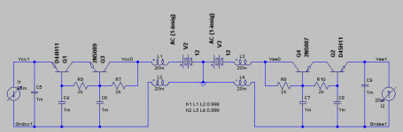
A few notes about this "bastardized" design. Matched the Vgs of jfets J1-J9 as close as I could. Chose J10, J11, so that their combined Idss would be a bit larger than the combined current through J1-J9. Then chose R3 to get the highest gain at node a11. The voltage at a11 is around 5V. Tested the circuit with LT1028A for U1, but the noise was the same, so I left the OP27 in.
At this point if I implement something I'd like it to be tried and true, like syn08's circuit. So that might be next for me.
Question to syn08: what kind of matching, selecting did you have to do with the bf862s to get below 0.3nV/rtHz at 1kHz?
Question to Samuel: did you achieve 0.3nV/rtHz with the design that you have pointed me to earlier?
1) to rule out that the noise comes from the PSU (batteries), I built a filter similar to the one syn08 uses in HPS 5.1. The noise was higher than with batteries, when powered from the lab psu, and the noise was the same when the filter was between batteries and the circuit
2) to check again that a passive load would have lower noise, I replaced the 2xJ310 CCS with wire wound resistors of various values and measured the noise at 1kHz. The lowest noise with a resistor load was about 0.51nV/rtHz.
3) to eliminate the noise from the second stage I disconnected R8 from node a11, and Rf2 from node out. Then measured the gain at a11 with the CCS and with the best resistor load. The gain with the CCS was about 39.4dB, and the measured input referred noise measured at 0.42nV/rtHz. The gain with the resistor load was 26.3dB and the input referred noise measured at 0.48nV/rtHz.
4) to check if the noise could be further reduced by paralleling more devices I tried 18x2sk170bl with various different loads optimized (CCS and passive). Could not get the noise below 0.43nV/rtHz.
The batteries were freshly charged.
A few notes about this "bastardized" design. Matched the Vgs of jfets J1-J9 as close as I could. Chose J10, J11, so that their combined Idss would be a bit larger than the combined current through J1-J9. Then chose R3 to get the highest gain at node a11. The voltage at a11 is around 5V. Tested the circuit with LT1028A for U1, but the noise was the same, so I left the OP27 in.
At this point if I implement something I'd like it to be tried and true, like syn08's circuit. So that might be next for me.
Question to syn08: what kind of matching, selecting did you have to do with the bf862s to get below 0.3nV/rtHz at 1kHz?
Question to Samuel: did you achieve 0.3nV/rtHz with the design that you have pointed me to earlier?
Attachments
Question to syn08: what kind of matching, selecting did you have to do with the bf862s to get below 0.3nV/rtHz at 1kHz?
Question to Samuel: did you achieve 0.3nV/rtHz with the design that you have pointed me to earlier?
None, zero, zip, nada, jack ****. Matching JFETs here is absolutely useless. Sorting for noise is a different story and I used my Quantech to sort the 2SK170 to 0.7-0.8nV/rtHz. No noise sorting for BF862.
I'm pretty confident you are not measuring white noise only. If there's no difference between LT1028 (0,85nV/rtHz) and OP27 (3nV/rtHz), then the first stage is doing a proper job. For a 1nV/rtHz opamp, a gain of 5 in the first stage is enough to make the opamp noise negligible. Your problem is in the power supply, low PSRR and EMI injection. The noise cancelling buffer is worse compared with batteries, not because it's noisier but because it has higher output impedance.
Is there no way some of them to current hog if wide apart in IDSS since there are no individual source resistors?
Hi Ikoflexer,
good experiments and useful data.
What is the noise floor of your analyser?
With the resistor load the gain is about 5x lower (39.4dB vs 26.3dB, or 100x vs 20x). If your analyser noise floor is not below 5nV/rtHz, it can account for the observed higher noise of 0.48nV/rtHz compared to 0.42nV/rtHz.
Assuming uncorrelated noise sources in the JFET's and the analyser (a fair assumption I'd say), the total noise is root of the sum of squares.
So measured noise is sqrt ( ( JFET_noise*gain)^2 + (analyser_noise)^2 ).
Suppose the JFET input referred noise is really 0.42nV/rtHz, and the analyser has 5nV/rtHz floor.
Then in case of CSS with 100x gain, the total measured noise would be: sqrt ( (0.42n*100)^2 + (5n)^2 ) = 0.423nV/rtHz
With the resistor with 20x gain, it would be: sqrt ( (0.42n*20)^2 + (5n)^2 ) = 0.488nV/rtHz
You could easily draw the wrong conclusion 😉
good experiments and useful data.
The gain with the CCS was about 39.4dB, and the measured input referred noise measured at 0.42nV/rtHz. The gain with the resistor load was 26.3dB and the input referred noise measured at 0.48nV/rtHz.
What is the noise floor of your analyser?
With the resistor load the gain is about 5x lower (39.4dB vs 26.3dB, or 100x vs 20x). If your analyser noise floor is not below 5nV/rtHz, it can account for the observed higher noise of 0.48nV/rtHz compared to 0.42nV/rtHz.
Assuming uncorrelated noise sources in the JFET's and the analyser (a fair assumption I'd say), the total noise is root of the sum of squares.
So measured noise is sqrt ( ( JFET_noise*gain)^2 + (analyser_noise)^2 ).
Suppose the JFET input referred noise is really 0.42nV/rtHz, and the analyser has 5nV/rtHz floor.
Then in case of CSS with 100x gain, the total measured noise would be: sqrt ( (0.42n*100)^2 + (5n)^2 ) = 0.423nV/rtHz
With the resistor with 20x gain, it would be: sqrt ( (0.42n*20)^2 + (5n)^2 ) = 0.488nV/rtHz
You could easily draw the wrong conclusion 😉
Jeepee, with the analyzer port shorted, the measurement at 1kHz is 10nV/rtHz (on average). When I reported for instance 0.43nV/rtHz for the CCS load, the analyzer actually showed 430nV/rtHz. The input referred noise would then be 430/1000nV/rtHz, so I reported 0.43.
I didn't even bother to subtract the analyzer noise floor. If I did, I should have reported a noise of sqrt (430^2 - 10^2) / 1000 = 429.88/1000 = 0.42988nV/rtHz input referred noise.
Does this make sense?
I didn't even bother to subtract the analyzer noise floor. If I did, I should have reported a noise of sqrt (430^2 - 10^2) / 1000 = 429.88/1000 = 0.42988nV/rtHz input referred noise.
Does this make sense?
Ikoflexer, yes it makes sense.
However, when you measured the input stage only, you reported 100x gain (39.4dB) so I guess you saw 43nV/rtHz on the analyser in that case, correct?
The 430nV/rtHz is with the full amplifier, including Opamp at 1000x (60dB), correct? Or did I misinterpret your postings.
With a 10nV/rtHz analyser noise floor, the CCS case with 100x gain (input stage only) or 1000x gain (full amp) has 0.43nV/rtHz equivalent input noise.
But the resistor load case with gain 20x you measured 0.48nV/rtHz, which is better than the noise floor of the analyser alone, referred to the JFET input: 10nV/rtHz/20=0.5nV/rtHz 😕
Measurements accuracies set aside, it would mean the resistor load case is much better than the CCS.
Maybe you can crank up the gain of the resistor load case with a higher drain resistor, say 4x higher, and four times the battery voltage (stacking 4 pieces)? Or maybe you have another 10x amp with noise floor well below the 10nV/rtHz of the analyser...
Ikoflexer, yes it makes sense.
However, when you measured the input stage only, you reported 100x gain (39.4dB) so I guess you saw 43nV/rtHz on the analyser in that case, correct?
The 430nV/rtHz is with the full amplifier, including Opamp at 1000x (60dB), correct? Or did I misinterpret your postings.
Yes indeed. I reported the noise divided by the gain of the particular stage that I measured.
With a 10nV/rtHz analyser noise floor, the CCS case with 100x gain (input stage only) or 1000x gain (full amp) has 0.43nV/rtHz equivalent input noise.
But the resistor load case with gain 20x you measured 0.48nV/rtHz, which is better than the noise floor of the analyser alone, referred to the JFET input: 10nV/rtHz/20=0.5nV/rtHz 😕
The analyzer noise floor shouldn't get divided by the gain, because it gets added directly to the very output of the preamp, right?
Measurements accuracies set aside, it would mean the resistor load case is much better than the CCS.
Maybe you can crank up the gain of the resistor load case with a higher drain resistor, say 4x higher, and four times the battery voltage (stacking 4 pieces)? Or maybe you have another 10x amp with noise floor well below the 10nV/rtHz of the analyser...
To me it appeared that the CCS load was better (lower noise) after normalizing for the different gains.
The analyzer noise floor shouldn't get divided by the gain, because it gets added directly to the very output of the preamp, right?
See your own post 330...
I didn't even bother to subtract the analyzer noise floor. If I did, I should have reported a noise of sqrt (430^2 - 10^2) / 1000 = 429.88/1000= 0.42988nV/rtHz input referred noise.
it's all about "equivalent INPUT referred noise", isn't it?
To me it appeared that the CCS load was better (lower noise) after normalizing for the different gains.
Normalize both cases again...
One could easily draw the wrong conclusion 😉
PS: maybe you can quote the actual analyser readings for the CSS and resistor. Also the gain and the voltage on the node "a11" in both cases. Node "a11" is the output node in this case, isn't it?
Last edited:
OK, sorry about the confusion. Let me try again.
Yes, it is.
I'll start first quoting myself from post 326. This experiment was intended to measure the first stage with both resistor and CCS load, so the second stage was completely disconnected.
To measure the noise the setup was as follows:
0R -> preamp -> analyzer 1Meg input -> analyzer screen
To measure the gain the setup was as follows:
a) 2.5mV RMS 1kHz sine wave from HP function generator -> true RMS voltmeter (Fluke 931B)
b) 2.5mV RMS 1kHz sine wave from HP function generator -> preamp -> true RMS voltmeter (Fluke 931B)
So gain is measured value from b) divided by measured value from a)
With the CCS the gain was 39.4dB which is approx. 93.3
With the resistor the gain was 26.3dB which is approx. 20.6
With the CCS, the measured noise at 1kHz (read on the analyzer screen) was about 39nV/rtHz. The HP 3585A analyzer has a "noise level" function which rreports the noise spectral density at the marker position (in this case 1kHz).
So I divided 39 by 93.3 to get 0.42nV/rtHz, the equivalent input referred noise of the preamp, ignoring the analyzer noise floor because I didn't think it was significant. If I had subtracted, the result would have been 37.7nV/rtHz = sqrt(39^2-10^2), or referred to the input, 37.7/93.3 = 0.4nV/rtHz.
Now, the resistor load case. The analyzer reported 14nV/rtHz at 1kHz. Because 14nV/rtHz was so close to the analyzer noise floor, I subtracted it. So
sqrt(14^2-10^2) = 9.8
which when divided by the gain of 20.6 results in 0.48nV/rtHz
This is the reason I said that to me it appears that the CCS load results in lower equivalent input referred noise than the resistor.
It is possible that I made a mistake though.
See your own post 330...
it's all about "equivalent INPUT referred noise", isn't it?
Yes, it is.
Normalize both cases again...
PS: maybe you can quote the actual analyser readings for the CSS and resistor. Also the gain and the voltage on the node "a11" in both cases. Node "a11" is the output node in this case, isn't it?
I'll start first quoting myself from post 326. This experiment was intended to measure the first stage with both resistor and CCS load, so the second stage was completely disconnected.
ikoflexer said:3) to eliminate the noise from the second stage I disconnected R8 from node a11, and Rf2 from node out. Then measured the gain at a11 with the CCS and with the best resistor load. The gain with the CCS was about 39.4dB, and the measured input referred noise measured at 0.42nV/rtHz. The gain with the resistor load was 26.3dB and the input referred noise measured at 0.48nV/rtHz.
To measure the noise the setup was as follows:
0R -> preamp -> analyzer 1Meg input -> analyzer screen
To measure the gain the setup was as follows:
a) 2.5mV RMS 1kHz sine wave from HP function generator -> true RMS voltmeter (Fluke 931B)
b) 2.5mV RMS 1kHz sine wave from HP function generator -> preamp -> true RMS voltmeter (Fluke 931B)
So gain is measured value from b) divided by measured value from a)
With the CCS the gain was 39.4dB which is approx. 93.3
With the resistor the gain was 26.3dB which is approx. 20.6
With the CCS, the measured noise at 1kHz (read on the analyzer screen) was about 39nV/rtHz. The HP 3585A analyzer has a "noise level" function which rreports the noise spectral density at the marker position (in this case 1kHz).
So I divided 39 by 93.3 to get 0.42nV/rtHz, the equivalent input referred noise of the preamp, ignoring the analyzer noise floor because I didn't think it was significant. If I had subtracted, the result would have been 37.7nV/rtHz = sqrt(39^2-10^2), or referred to the input, 37.7/93.3 = 0.4nV/rtHz.
Now, the resistor load case. The analyzer reported 14nV/rtHz at 1kHz. Because 14nV/rtHz was so close to the analyzer noise floor, I subtracted it. So
sqrt(14^2-10^2) = 9.8
which when divided by the gain of 20.6 results in 0.48nV/rtHz
This is the reason I said that to me it appears that the CCS load results in lower equivalent input referred noise than the resistor.
It is possible that I made a mistake though.
None, zero, zip, nada, jack ****. Matching JFETs here is absolutely useless. Sorting for noise is a different story and I used my Quantech to sort the 2SK170 to 0.7-0.8nV/rtHz. No noise sorting for BF862.
I'm pretty confident you are not measuring white noise only. If there's no difference between LT1028 (0,85nV/rtHz) and OP27 (3nV/rtHz), then the first stage is doing a proper job. For a 1nV/rtHz opamp, a gain of 5 in the first stage is enough to make the opamp noise negligible. Your problem is in the power supply, low PSRR and EMI injection. The noise cancelling buffer is worse compared with batteries, not because it's noisier but because it has higher output impedance.
Thank you. In an attempt to improve the PSRR and get rid of some of the RF junk I implemented this simple cap multiplier (Joachim, good suggestion!). Also added a common mode ferrite choke like those found in the psu of many CRT monitors. This filter made a difference in powering the circuit from the lab supply which is terribly noisy. It cleaned up most of the junk. The filter output impedance is dismal, so I may come up with some filter/regulator that's better than this one.
One issue might be the filter self-noise, hence I used the D4xH11 in that position, which seemed to be more sensitive.
Now, with the preamp input shorted, and powered from the lab psu, the equivalent input referred noise was almost as low as when using batteries. In fact the difference is so small that I'm not sure. For me this is a bit of progress because I can live with a tiny bit higher noise than using batteries, but get rid of the nonsense of recharging.
Attachments

Reverse the leads to one winding of the common mode choke.
Good catch, thank you Joachim.
Attachments
- Home
- Amplifiers
- Solid State
- Simple 60dB discrete low noise amplifier (lna)