He uses 32dB gain as standard he mentioned.
The circuit he posted earlier has 60dB gain. I have no doubt this kind of thing is trivial for syn08 and Samuel. It's probably really frustrating to them to see what I'm doing.
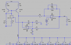
jeepee, I'm not sure if this is what you had in mind? I'll read your post again more carefully.
Edit: actually I'm sure I got it wrong.
Attachments
Hi Ikoflexer,
well done, you translated my "netlist in words" to the schematic I had in mind (literally). Are the results satisfactory? What's the voltage on node a11?
Your late night experiment with dissapointing noise, points again to the fact that whatever you put on the drain side of the input JFET's, is simply in parallel to that input JFET drain current noise. So it adds up and spoils your ultra low noise input stage performance...
Can you simulate the noise of your circuit(s)? Just for fun, take you simple schematic, the one with the 150 Ohm Rdrain and make the supply 10x higher and the drain resistor 10x150 Ohm, what happens to the noise? Try again with 100x supply and resistor value. Don't change the OpAmp supply though 🙂
So what I don't understand well is why the BD140 current mirror would have such higher noise, whereas the simple 2xJ310 CCS achieved the lowest noise.
Ikoflexer, try again with 150 Ohm degeneration...
BTW: that late night circuit, even though AC coupled, still has the "fighting" current sources... You need to "slave" the upper current source one way or the other. There is no degree of freedom in that circuit. Loopgain is not important, since the input JFET drain (signal) current is sinked (sunk) by the near 0 Ohm small signal input impedance of the transimpedance stage (U1/R12). The circuit is a concatenation of a transadmittance stage, V-to-I [JFET J1-J9], and a transimpedance stage, I-to-V [U1/R12]. Open Loopgain is gm_JFET*R12. At the intermedaite node, a11, there is ideally no signal voltage. The signal is in the current domain.
Edit: actually I'm sure I got it wrong.
PS: don't forget to increase the VCC by +2V, or reduce R5/R6 a little (120/1080 Ohm) to allow enough voltage headroom for Q1 and J10.
Hi Ikoflexer,
well done, you translated my "netlist in words" to the schematic I had in mind (literally). Are the results satisfactory? What's the voltage on node a11?
With 3V on the +IN of U1, the DC voltage at a11 is 4.09V. V(out) is -10V. The currents through the current mirror are totally out of whack!
I think this isn't working exactly as you wanted. Let's see if I understood what we want here. We want the CCS DC current to be as close as possible to the jfet Id. Don't we then want to sense the DC jfet current and then via feedback of some sort manipulate the current mirror to deliver something close to that?
Your late night experiment with disapointing noise, points again to the fact that whatever you put on the drain side of the input JFET's, is simply in parallel to that input JFET drain current noise. So it adds up and spoils your ultra low noise input stage performance...
Yes, it just isn't clear to me why 2xJ310 would be less noisy than the BD140 mirror. The J310 is rated at about 6nV/rtHz I think. Perhaps the BD140 setup has quite a bit more current noise.
Can you simulate the noise of your circuit(s)? Just for fun, take you simple schematic, the one with the 150 Ohm Rdrain and make the supply 10x higher and the drain resistor 10x150 Ohm, what happens to the noise? Try again with 100x supply and resistor value. Don't change the OpAmp supply though 🙂
Jeepee, ltspice has a "noise" analysis but I wouldn't trust it at all. I think it does only very basic thermal noise analysis.
It's probably really frustrating to them to see what I'm doing.
Yes it is, mostly because it's a ******* moving target. Why on earth are you looking for DC coupling in the gain stage (and servo, etc...) when you are coupling the source in AC via a cap? If you are happy with AC, just put a film cap between the first and second stage, and voila, no more servo required.
You were told by three different people that the servo, as you stubbornly trying to use, won't ever work. The CCS and the JFETs are fighting for current and the output will either flip or motorboat, in any practical implementation.
And why in hell do you insist on a CCS load, when you were already shown other multiple solutions to increase the PSRR? To increase the loop gain? Flashews, that comes at the price of phase margin, there is no free lunch. To increase the PSRR? That comes to the price of added noise. The J310 CCS went better not because any magic with the JFETs, but because it was working as a gate controlled resistor rather than a CCS, both Samuel and myself mentioned this several times, being as effective as any metal film load resistor. And finally, exactly how much PSRR are you looking for?
Make sure you tell anybody what you are doing. Is it simulation, or tin can air breadboarding? Are you measuring or simulating the numbers? When something doesn't work properly, just make sure you understand why, rather then dismissing a possibly otherwise perfectly good solution.
You are not happy with 0.4nV/rtHz, well flashnews, that's about all you can do with 8x2SK170 not sorted for noise. 1nV/rtHz/SQRT(8)=0.35nV/rtHz. Get BF862 with 0.8nV/rtHz and you may have a better chance.
You complain about closed loop gain not being exactly 60dB, well check your gain setting components for precision and your measurement setup for errors, because that thing has over 100,000 loop gain Errors should be well under 1% (the regular resistor precision).
You complain about bipolar CCS being noisy, yes sir, bipolars have current noise and the current noise in the CCS modulates the precious gain current.
And last but not the least, you want to build an ultra low noise, high gain amplifier in a tin can, that is anything but good shielding against RFI. And complain about stability issues when you were already told several times that parasitic inductances are critical.
Stop farting around, decide for the requirements, write them down, post them and then people can make an educated guess for the best solution, without much guessing. Put your money where your mouth is and design+build a proper (shielding, grounding, etc...) PCB. Clean and calibrate your measurement setup, evaluate the error sources, then measure your construction. It doesn't work properly? Well tough ****, draw the conclusions/lessons learned and start over.
Last edited:
PS: don't forget to increase the VCC by +2V, or reduce R5/R6 a little (120/1080 Ohm) to allow enough voltage headroom for Q1 and J10.
I have indeed increased Vcc to 15V, but still doesn't work. The operating points of the first stage are broken.
IKO, you must KILL the Gm of the current mirror transistors. Larger R in the emitters is better than less R. This is the key. The current mirror and any other active load, AMPLIFIES its own noise, just like an added source.
syn08, I don't even know what to say to you. Instead of addressing each point, I'll just go for a blurb. Please understand that I have a few objectives here. One is to eventually end up with a preamp that works. The other is to explore and learn, hence the moving target. I'm quite happy with 0.4nV/rtHz, but hey, why not push it as far as it goes?
I don't think I dismissed any suggestions so far. Out of respect for the time other people took to make a suggestion I make a point out of putting the time to test it. For every suggestion, first I plug it in the simulator, more to capture the schematic but also for basic sanity tests. Then I built it in the tin can. Why do you insist on a pcb? I could argue that using a pcb will add noise. Let's see if you laugh 🙂 In any case, I don't want to argue, I do what I can. You have the benefit of EE schooling. I don't. Think of what I do as "EE lab 101." I appreciate your input and followed your advice as well as I could.
I don't think I dismissed any suggestions so far. Out of respect for the time other people took to make a suggestion I make a point out of putting the time to test it. For every suggestion, first I plug it in the simulator, more to capture the schematic but also for basic sanity tests. Then I built it in the tin can. Why do you insist on a pcb? I could argue that using a pcb will add noise. Let's see if you laugh 🙂 In any case, I don't want to argue, I do what I can. You have the benefit of EE schooling. I don't. Think of what I do as "EE lab 101." I appreciate your input and followed your advice as well as I could.
To start over, you were given two solutions that were experimented and are proven as working properly. You dismissed both as being "unstable". Well, they are both (Samuel's and mine) rock solid and the only reason why your isn't is, guess what, the tin can construction. Now, if you add to the requirements "to be feasible for a tin can construction" then I can't certainly help (and I guess nobody can make anything but an educated guess).
However, because you took the time, I should take the time to answer.
You're right, I didn't and wouldn't care much for a servo. But the servo (in simulation) seemed to have better gain at low frequency, unless a really large cap would be used in the AC coupling. I will try it, and if it works, I'll stay with AC coupling.
Yes, but I wanted to try it and see how it fails.
I don't insist on a CCS load, but wanted to explore this idea, partly to increase the loop gain of the first stage.
It was my impression that the first stage should have enough gain so that its noise would dominate the total noise of the preamp. One things that I don't understand in this transimpedance amplifier + feedback is how the gain of the first stage is maintained as high as possible, when in the same time the feedback is applied to the jfet source, and also the gain is set roughly by gm*opamp_feedback_resistor. So, in trying to understand this, I wanted to see what happens trying to get the highest gain possible from the first stage (using a CCS load).
The 2xJ310 not a CCS but working as a gate controlled resistor. I guess you use the term CCS to refer to an ideal CCS? Whatever it is, I got higher first stage gain and lower overall noise using the 2xJ310 than with any resistor. And believe me, I've tried to come up with the best value load resistor. If the J310 was just a resistor, I should have been able to replace it with another resistor or proper value. The way I think about it is that the 2xJ310 is nearer a CCS than a simple resistor.
I have done both, simulation just for sanity checks, and if passed, implemented all of it in a tin can. With lid, and with the batteries inside. I know it's not perfect shielding, but it is enough shielding for prototyping. Indeed, when I bring the tin can near the analyzer or the oscilloscope, the noise increases. So all the numbers I reported were measured with the noise level function of the HP 3585A, at 1kHz. I thought I said that before.
I definitely agree with you that some suggestions might be excellent, but my implementation is wrong. Well, I do my best. Possible that mistakes happen, of course. Yes, I do try to understand why things don't work, or work.
Not that I'm not happy, but it's fun to try for better. Surely you understand that. Now that mouser has the bf862 in stock again, will get some. I tell what I'm not very happy with. That they come in the sot23 package and it's not as easy to match and prototype with them.
I have used 0.1% tolerance resistors, double checked with a GenRad RLC bridge.
Hey, easy, I'm a beginner. I'm just finding things out here. To me it's fun to find things out doing real circuits, rather than just reading it in a book.
I had stability problems mainly when using the LT1028. Here I don't disagree with you.
So you're saying that if I build your exact circuit using bf862 and the opamp you use, and even use your pcb design, and then put it in a thick steel case, it will be stable and it will work 100% as it should?
You see, sometimes I'm afraid to invest so much energy in something that I'm not 100% it will work. Also, building your circuit only, if it works, I just learn to solder and build a case.
At some point I will do that. For now, I will explore different ideas and fool around. If what I do bothers you, just ignore my fooling around.
Yes it is, mostly because it's a ******* moving target. Why on earth are you looking for DC coupling in the gain stage (and servo, etc...) when you are coupling the source in AC via a cap? If you are happy with AC, just put a film cap between the first and second stage, and voila, no more servo required.
You're right, I didn't and wouldn't care much for a servo. But the servo (in simulation) seemed to have better gain at low frequency, unless a really large cap would be used in the AC coupling. I will try it, and if it works, I'll stay with AC coupling.
You were told by three different people that the servo, as you stubbornly trying to use, won't ever work. The CCS and the JFETs are fighting for current and the output will either flip or motorboat, in any practical implementation.
Yes, but I wanted to try it and see how it fails.
And why in hell do you insist on a CCS load, when you were already shown other multiple solutions to increase the PSRR? To increase the loop gain? Flashews, that comes at the price of phase margin, there is no free lunch. To increase the PSRR? That comes to the price of added noise. The J310 CCS went better not because any magic with the JFETs, but because it was working as a gate controlled resistor rather than a CCS, both Samuel and myself mentioned this several times, being as effective as any metal film load resistor. And finally, exactly how much PSRR are you looking for?
I don't insist on a CCS load, but wanted to explore this idea, partly to increase the loop gain of the first stage.
It was my impression that the first stage should have enough gain so that its noise would dominate the total noise of the preamp. One things that I don't understand in this transimpedance amplifier + feedback is how the gain of the first stage is maintained as high as possible, when in the same time the feedback is applied to the jfet source, and also the gain is set roughly by gm*opamp_feedback_resistor. So, in trying to understand this, I wanted to see what happens trying to get the highest gain possible from the first stage (using a CCS load).
The 2xJ310 not a CCS but working as a gate controlled resistor. I guess you use the term CCS to refer to an ideal CCS? Whatever it is, I got higher first stage gain and lower overall noise using the 2xJ310 than with any resistor. And believe me, I've tried to come up with the best value load resistor. If the J310 was just a resistor, I should have been able to replace it with another resistor or proper value. The way I think about it is that the 2xJ310 is nearer a CCS than a simple resistor.
Make sure you tell anybody what you are doing. Is it simulation, or tin can air breadboarding? Are you measuring or simulating the numbers? When something doesn't work properly, just make sure you understand why, rather then dismissing a possibly otherwise perfectly good solution.
I have done both, simulation just for sanity checks, and if passed, implemented all of it in a tin can. With lid, and with the batteries inside. I know it's not perfect shielding, but it is enough shielding for prototyping. Indeed, when I bring the tin can near the analyzer or the oscilloscope, the noise increases. So all the numbers I reported were measured with the noise level function of the HP 3585A, at 1kHz. I thought I said that before.
I definitely agree with you that some suggestions might be excellent, but my implementation is wrong. Well, I do my best. Possible that mistakes happen, of course. Yes, I do try to understand why things don't work, or work.
You are not happy with 0.4nV/rtHz, well flashnews, that's about all you can do with 8x2SK170 not sorted for noise. 1nV/rtHz/SQRT(8)=0.35nV/rtHz. Get BF862 with 0.8nV/rtHz and you may have a better chance.
Not that I'm not happy, but it's fun to try for better. Surely you understand that. Now that mouser has the bf862 in stock again, will get some. I tell what I'm not very happy with. That they come in the sot23 package and it's not as easy to match and prototype with them.
You complain about closed loop gain not being exactly 60dB, well check your gain setting components for precision and your measurement setup for errors, because that thing has over 100,000 loop gain Errors should be well under 1% (the regular resistor precision).
I have used 0.1% tolerance resistors, double checked with a GenRad RLC bridge.
You complain about bipolar CCS being noisy, yes sir, bipolars have current noise and the current noise in the CCS modulates the precious gain current.
Hey, easy, I'm a beginner. I'm just finding things out here. To me it's fun to find things out doing real circuits, rather than just reading it in a book.
And last but not the least, you want to build an ultra low noise, high gain amplifier in a tin can, that is anything but good shielding against RFI. And complain about stability issues when you were already told several times that parasitic inductances are critical.
I had stability problems mainly when using the LT1028. Here I don't disagree with you.
So you're saying that if I build your exact circuit using bf862 and the opamp you use, and even use your pcb design, and then put it in a thick steel case, it will be stable and it will work 100% as it should?
You see, sometimes I'm afraid to invest so much energy in something that I'm not 100% it will work. Also, building your circuit only, if it works, I just learn to solder and build a case.
Stop farting around, decide for the requirements, write them down, post them and then people can make an educated guess for the best solution, without much guessing. Put your money where your mouth is and design+build a proper (shielding, grounding, etc...) PCB. Clean and calibrate your measurement setup, evaluate the error sources, then measure your construction. It doesn't work properly? Well tough ****, draw the conclusions/lessons learned and start over.
At some point I will do that. For now, I will explore different ideas and fool around. If what I do bothers you, just ignore my fooling around.
To start over, you were given two solutions that were experimented and are proven as working properly. You dismissed both as being "unstable". Well, they are both (Samuel's and mine) rock solid and the only reason why your isn't is, guess what, the tin can construction. Now, if you add to the requirements "to be feasible for a tin can construction" then I can't certainly help (and I guess nobody can make anything but an educated guess).
OK, I will build your exact circuit and will put it in a thick steel case, or whatever case you suggest. I owe you this much. But will also fool around with my things, which you can ignore. 🙂
OK, I will build your exact circuit and will put it in a thick steel case, or whatever case you suggest. I owe you this much. But will also fool around with my things, which you can ignore. 🙂
You don't have to, I doubt you can directly copy my design layout (it's integrated in the RIAA pre, it's SMD (so no easy prototyping) and has a different gain) and BTW, you don't owe me anything.
Trying to understand why the thing was not stable in your implementation is the right way to go, if you want to learn something useful. Get the schematic, simulate the loop gain, add parasitics and watch the impact, etc... Possible suggestions: if my design was motorboating, try go down from 150ohm to 120ohm or 100ohm (first stage load resistor). While powering up, the output flips to the rails and it takes a few seconds to stabilize to zero. If this flipping transiently saturates the cascode transistor, it may trigger motorboating. Or lower the servo integrator cap to 0.1uF (instead of 1uF).
Otherwise, shooting everywhere and changing every bit of the design won't create anything but confusion for yourself, those trying to help, and the readers looking forward to learn something. Chances are high you will end up with a bastardized design that nobody will be able understand and to reproduce. This approach is usually called "disciplined".
Otherwise, shooting everywhere and changing every bit of the design won't create anything but confusion for yourself, those trying to help, and the readers looking forward to learn something. Chances are high you will end up with a bastardized design that nobody will be able understand and to reproduce. This approach is usually called "disciplined".
Indeed. Making one approach work and approach its theoretical performance will be much more helpful for your learing experience than randomly trying out various topologies which you haven't understud.
If I design something like this (yes I have built 300 pV/sqrt(Hz) amps) the design procedure is typically about as follows:
* Set the design goals. This includes numerous things such as voltage and current noise, gain, frequency response, input impedance, common-mode rejection (for balanced inputs), power supply voltage and current, power supply rejection, ground isolation, parts cost/complexity and available design time/number of design cycles. These goals might need some slight revision later (if there's no customer which pays you) if you see that a trade-off is required but you can't randomly jump between 0.1 nV/sqrt(Hz), 1 nV/sqrt(Hz), 10k input Z and 10M input Z.
* Evaluate possible input transistors, their optimum operating conditions and the number of paralleled devices required. The transistors should mainly offer low voltage/current noise and high gm. This should be achieved at low bias current and low operating voltage to reduce sensitivity to thermal gradients (which cause drift and 1/f noise) and to simplify the design of the second stage.
* Evaluate possible amplifier topologies compatible with the design goals and the chosen input transistors. Usually there are only a handful of known topologies to chose from; evaluate them by consideration of prior art amplifiers (is there any amp which already comes close to your goals?) and pen & paper work. Simulation (at this level I work mostly with idealised components, e.g. opamps, voltage sources and current source) reduces the amount of math to be done by hand but is only of limited help in understanding the basic operation of the topology and the trade-offs involved.
* Draw a (perhaps somewhat simplified) pen & paper schematic using the most promising amplifier topology. Work out all bias conditions, the values of the passives (e.g. for compensation and frequency response) and the choice of other components (opamps, diodes etc.).
* Run a thorough simulation of the design. Estimate how valid the simulation result is (e.g. does it depend on exact and/or matching transistor parameters? Are the used models sufficiently accurate?). Redesign if necessary.
* If necessary evaluate sub-circuits for which theoretical results are doubtful in real world. A typical example might be the voltage noise of a zener diode, excess noise of a critical resistor or the stability of a discrete output buffer. Redesign if necessary.
* Build a prototype. With higher complexity, higher bandwidth (i.e. sensitivity to parasitics) and more demanding specifications the need for a PCB-based prototype increases. Make sure the prototype has correct bias conditions and is stable.
* Evaluate the prototype for all design goals. Be very critical regarding measurement validity. For my work I've found that 3 out of 4 times I need to rework the measurement procedure, not the design.
* If one or more goals are not met find out where theory doesn't fit real world. This can be the most difficult and time consuming design step. Don't fall into the trap of randomly applying changes to your circuit; instead re-evaluate assumptions, simulation results and datasheet values. Simplify by isolated consideration of sub-circuits.
* Iteratively apply the above steps...
Samuel
Last edited:
This is an FFT of the Colin amp @ 100X averaged 256X -- the power spectrum even with the AP input shorted shows some 60Hz energy picked, the cyan is with the amplifier off -- demonstrating that the box and associated 50 ohm cable are a good antenna for the energy coming from various radiators!
An externally hosted image should be here but it was not working when we last tested it.
IKO, I am going to give you yet another 'guide' to low noise design.
First, 0.3nV/rt Hz is the equivalent noise of a 5 ohm resistor, 0.4nV/rt Hz is eq. to 10 ohms, and 1nV/rt Hz is 60 ohms approximately.
For whatever reason: the EQUIVALENT R for a resistor is about .7/Gm of the total group of paralleled fets that you use. This is the best case, usually it is a little worse, because of biasing resistors and 1/f noise.
That comes out to about 25 ohms for a single 170 j-fet. Could be a little more, could be a little less, depending on devices and operating current. More current gives more Gm and lower noise, UNTIL the junction gets too hot. Paralleling 8 devices gives an ideal effective noise of 3+ ohms and with the added 1 ohm feedback resistor, it is theoretically possible to get 0.3nV/rt Hz.
Now, what is wrong?
First, current source loads can be very noisy, and usually add something significant. Why just not limit your design to a resistive load, either wirewound or a very high quality metal film resistor. This will not AMPLIFY its own noise, at least, although, make sure that you get a voltage gain on the input stage of at least 10, hopefully more in order to not have the second stage contribute much to the total. Just remember:
Vg>10=(Gm)(Rl). It is necessary to drop a few volts across the resistor be able to use a fairly high value with the given high current, and get you safely out of the added noise zone. Start, for example, with 100 ohms and see. Still, .4nV/rt Hz is pretty respectable.
This is a little bit clearer -- you can grab a beer between averaging the analyzer -- the SSM2019 has fewer issues with 1/f noise than the Colin Low Noise amp. (The case in which this SSM2019 is housed appears a little problematic.) I used the AP "equiripple" window, and averaged 256X.
The Colin amp, an LSK389 followed by an AD797 yields 1.9nV @10kHz, but 7.0nV @100 Hz. The SSM2019 @60dB is 3.1nV +/- 0.1nV down to 20Hz. The SSM2019 is least noisy at +60dB.
The thing which I will have to do is get your final design, put one together, and compare the lot. I think that the analyzer in analog bandpass mode may be better for low noise signals, but in digital mode you can see the problems in the low end of the range.
An externally hosted image should be here but it was not working when we last tested it.
IKO, I am going to give you yet another 'guide' to low noise design.
First, 0.3nV/rt Hz is the equivalent noise of a 5 ohm resistor, 0.4nV/rt Hz is eq. to 10 ohms, and 1nV/rt Hz is 60 ohms approximately.
For whatever reason: the EQUIVALENT R for a resistor is about .7/Gm of the total group of paralleled fets that you use. This is the best case, usually it is a little worse, because of biasing resistors and 1/f noise.
That comes out to about 25 ohms for a single 170 j-fet. Could be a little more, could be a little less, depending on devices and operating current. More current gives more Gm and lower noise, UNTIL the junction gets too hot. Paralleling 8 devices gives an ideal effective noise of 3+ ohms and with the added 1 ohm feedback resistor, it is theoretically possible to get 0.3nV/rt Hz.
Now, what is wrong?
Good question. I'm pretty sure I eliminated the second stage as a possible suspect. Today I've replaced the op07 with an lt1028 and the measurement remained around 0.43nV/rtHz.
First, current source loads can be very noisy, and usually add something significant. Why just not limit your design to a resistive load, either wirewound or a very high quality metal film resistor.
Two things about this. One, before trying the current source load I used a wirewound resistor. Its values was between 100 and 150 ohms; tried several values and chose that which gave me highest gain in the first stage, which amounted to around 30dB.
Then I tried a current source more out of curiosity; turned out that two paralleled J310 brought the overall noise down to less than 0.5nV/rtHz. Lower noise than with the resistor. Checked the gain of the first stage with this simple current source load, and it was, depending on its setup, between 40dB and 60dB. I didn't bother to look for the resistor that would give the highest gain here. Just as well, since I've been told (above) that trying to get high gain in this first stage is a mistake on my part.
In any case, the 9x2sk170bl jfets run at about 55mA DC. So I roughly matched a pair of J310 jfets to have a total Idss of more than 60mA, so that the right source-gate resistor would bring Id close to that of the paralleled 2sk170. So the J310 is rated at about 6nV/rtHz voltage noise. Two in parallel would have about 4.25nV/rtHz.
Something I don't understand well is why the noise of the J310 isn't affecting the overall noise more, and I don't understand why I was discouraged to get higher gain in the first stage.
This will not AMPLIFY its own noise, at least, although, make sure that you get a voltage gain on the input stage of at least 10, hopefully more in order to not have the second stage contribute much to the total. Just remember:
Vg>10=(Gm)(Rl). It is necessary to drop a few volts across the resistor be able to use a fairly high value with the given high current, and get you safely out of the added noise zone. Start, for example, with 100 ohms and see. Still, .4nV/rt Hz is pretty respectable.
I think 0.4nV/rtHz is just me fooling around with parts soldered in a tin can (and inadvertently frustrating the engineers with my undiscipline). Stable, solid, precise 60dB gain with 0.1nV/rtHz, out of a jfet input preamp with high psrr would be respectable. 🙂
You know IKO, this sort of circuit was first used, (by me) more than 40 years ago. It is not new, unique, or original. It is obvious. Now, when it comes to current sources, you just don't understand what you are doing, and I am having a hard time trying to find a way to explain it. I made the same mistake in 1968, when I tried to put a current source on my input stage in my Ampex master recorder. It got more noisy! You have the same basic problem. It is difficult to make a good current source that is quiet and has little residual Gm. Gm Rl works both ways, and you MUST dominate with a very high Gm from your input and low Gm from your current source. You are close, but not perfect. .1nV/rt Hz is absurd, without more j-fets.
- Home
- Amplifiers
- Solid State
- Simple 60dB discrete low noise amplifier (lna)