it was simply a way to derive a basic signal for feedback to the inverting input of the power amp. eventually I will recall the name of the company, although some other companies tried the scheme as well.
I'll put here the drawing Board to the soft start and protect the amplifier. This file is drawn in the program Sprint-Layout 6.
Attachments
Last edited:
I gave this file in the source program in order to be able to change under your terms, dimensions, or components.
Thanks again!I'll put here the drawing Board to the soft start and protect the amplifier. This file is drawn in the program Sprint-Layout 6.
I have a question,i see two inputs R.L from amplifier out but i see only one set of relays. Each of the relay disconnect different channel?
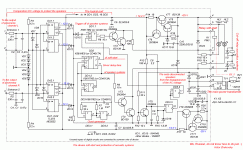
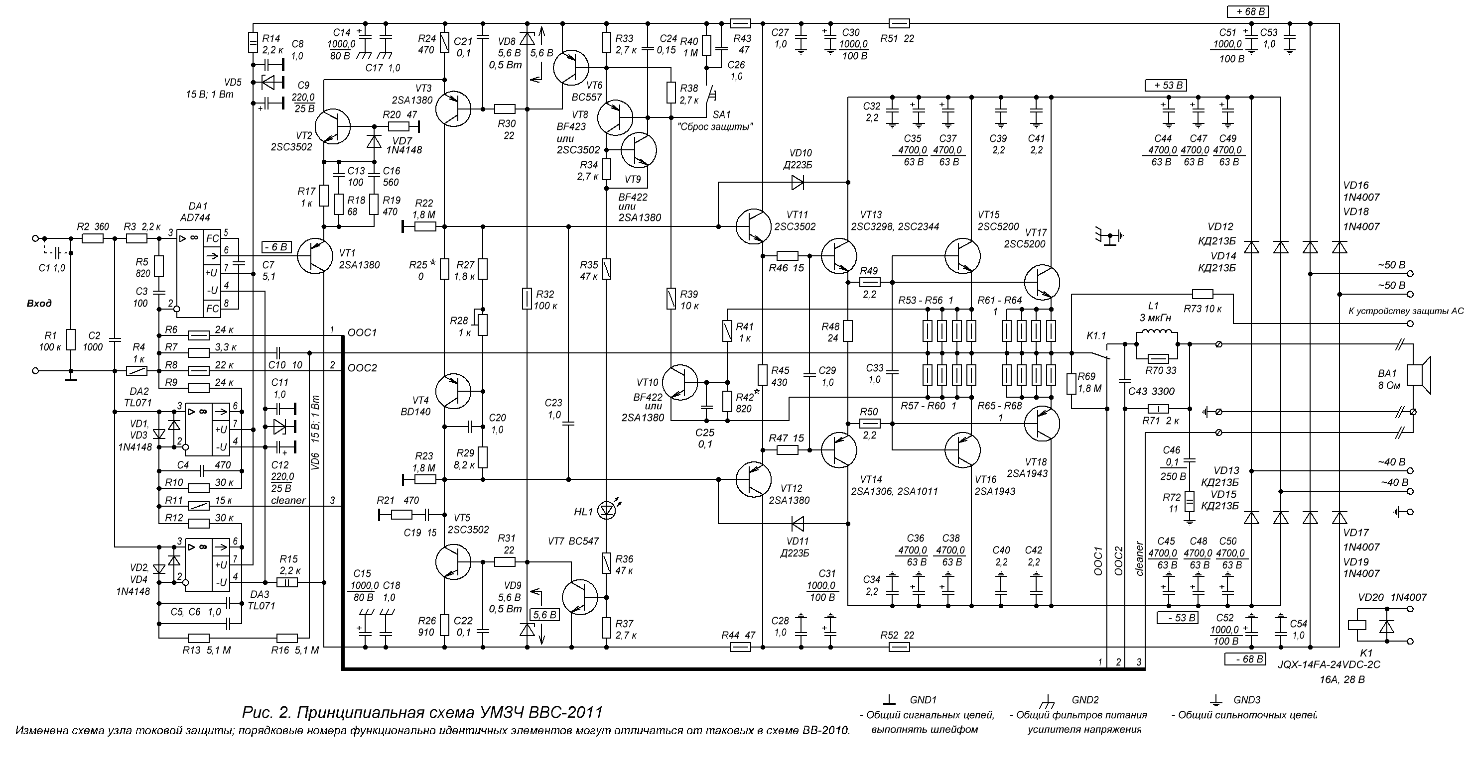
Electrical diagram has two cut outs for speakers for two channels. These relays mounted on PCB amps.
I did so, because during the flow of non-linear current speaker through the resistance of the relay contacts, the voltage drop across these contacts is also nonlinear. This nonlinear voltage drop is subtracted from the line voltage of the useful signal. Therefore, the voltage at the output terminals of the amplifier is distorted.
The value of the THD at lower frequencies (taking into account the resistance of the inductor at the output of the amplifier and impedance of acoustic systems) can reach 0,3%. This deterioration of linearity and sound occurs in all amps, that use relays to protect speakers.
The relay contacts in my amps covered with loop NFB to reduce distortion at the output terminals of the amplifier to less than one ppm. To about 0.000,15 - 0.000,3%% for different amplifiers. Many of these amplifiers are presented in this topic.
Therefore, the relay mounted on PCB amps. This solution allows to reduce the size of the loop NFB and interference on the wires of the NFB.
For example, in this picture:
http://www.diyaudio.com/forums/attachments/solid-state/548293d1462871663-several-schemes-2011.gif
http://www.diyaudio.com/forums/solid-state/290970-several-schemes.html
in the right part of the amplifier output, shows the contacts of the relay K1.1 (amplifier off) and the waste from these leads ООС1 and ООС2 two NFB loops. Loop NFB-1 ООС1 works from the moment you turn on the amplifier before the end of the time delay unit protection. When relay K1 is activated, the circuit turns off ООС1, loop NFB-2 ООС2 covers through the filter R71C43 the resistance of the relay contacts K1.1 and the resistance of the coil L1.
This may seem complex, but this diagram this is easy to assemble and it works perfectly. Sound is improved very clearly, you don't need to spend big money on thick wire to the speakers.
The voltage drop across the resistance of the wires of the acoustic system is measured by the unit of opamp DA3 through the wire "cleaner". This wire is connected to the "cold" terminal of the speaker system. The voltage drop at the "cold" wire of the speaker cable increases DA3 2 times (R10R11), the increased voltage is supplied to the main circuit NFB through R9.
The effect of operation of this unit is equivalent to connecting the amp directly to the speakers without cables.
Of course, the language barrier will prevent you to understand me so well as I would like. But you try to understand. It is very important to ensure that you had a good amplifier.
Last edited:
T117:
the specs are impressive.
thanks for sharing.
would you mind showing PCB layout, wiring and other constructional details about the unit having these measurement results? i think it would be educational.
thanks,
mlloyd1
the specs are impressive.
thanks for sharing.
would you mind showing PCB layout, wiring and other constructional details about the unit having these measurement results? i think it would be educational.
thanks,
mlloyd1
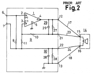
The amplifier in this diagram: http://www.diyaudio.com/forums/attachments/solid-state/548293d1462871663-several-schemes-2011.gif is simple and shows good results: http://www.diyaudio.com/forums/attachments/solid-state/548300d1462871663-several-schemes-19-20.jpg. For this circuit we built a lot of amplifiers. His diagram checked in LTSpice IV, all data of this program are confirmed - i.e., no unpredictability, a complete certainty. You can consider it for advertising: the engineers at Linear Technology was written by excellent software, they did a good job.
....
Never mind,
I see there are some additional photos in the beginning of the thread.
I didn't see images previously.
I'll review those and might have more questions later.
mlloyd1
I see there are some additional photos in the beginning of the thread.
I didn't see images previously.
I'll review those and might have more questions later.
mlloyd1
T117:
the specs are impressive.
thanks for sharing.
would you mind showing PCB layout, wiring and other constructional details about the unit having these measurement results? i think it would be educational.
thanks,
mlloyd1
Don't worry, all are clear now!Electrical diagram has two cut outs for speakers for two channels. These relays mounted on PCB amps.
I did so, because during the flow of non-linear current speaker through the resistance of the relay contacts, the voltage drop across these contacts is also nonlinear. This nonlinear voltage drop is subtracted from the line voltage of the useful signal. Therefore, the voltage at the output terminals of the amplifier is distorted.
The value of the THD at lower frequencies (taking into account the resistance of the inductor at the output of the amplifier and impedance of acoustic systems) can reach 0,3%. This deterioration of linearity and sound occurs in all amps, that use relays to protect speakers.
The relay contacts in my amps covered with loop NFB to reduce distortion at the output terminals of the amplifier to less than one ppm. To about 0.000,15 - 0.000,3%% for different amplifiers. Many of these amplifiers are presented in this topic.
Therefore, the relay mounted on PCB amps. This solution allows to reduce the size of the loop NFB and interference on the wires of the NFB.
For example, in this picture:
http://www.diyaudio.com/forums/attachments/solid-state/548293d1462871663-several-schemes-2011.gif
http://www.diyaudio.com/forums/solid-state/290970-several-schemes.html
in the right part of the amplifier output, shows the contacts of the relay K1.1 (amplifier off) and the waste from these leads ООС1 and ООС2 two NFB loops. Loop NFB-1 ООС1 works from the moment you turn on the amplifier before the end of the time delay unit protection. When relay K1 is activated, the circuit turns off ООС1, loop NFB-2 ООС2 covers through the filter R71C43 the resistance of the relay contacts K1.1 and the resistance of the coil L1.
This may seem complex, but this diagram this is easy to assemble and it works perfectly. Sound is improved very clearly, you don't need to spend big money on thick wire to the speakers.
The voltage drop across the resistance of the wires of the acoustic system is measured by the unit of opamp DA3 through the wire "cleaner". This wire is connected to the "cold" terminal of the speaker system. The voltage drop at the "cold" wire of the speaker cable increases DA3 2 times (R10R11), the increased voltage is supplied to the main circuit NFB through R9.
The effect of operation of this unit is equivalent to connecting the amp directly to the speakers without cables.
Of course, the language barrier will prevent you to understand me so well as I would like. But you try to understand. It is very important to ensure that you had a good amplifier.
Thanks.
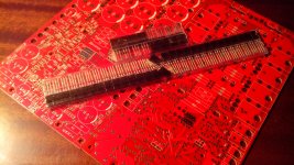
P.S Post the pcb for your amplifier if you want to see other guys making this.
Well.
The figure shows one side PCB. The second side is filled with a continuous layer of copper. This layer acts as a screen against interference from repeaters powerful output with large nonlinear currents. The protective layer is connected to the ground point GND (common Mecca).
Industrial quality PCB can be ordered here: aleanu@gmail.com. These PCB will look like this:

http://s019.radikal.ru/i623/1610/20/d6246e91dcff.jpg
The figure shows one side PCB. The second side is filled with a continuous layer of copper. This layer acts as a screen against interference from repeaters powerful output with large nonlinear currents. The protective layer is connected to the ground point GND (common Mecca).
Industrial quality PCB can be ordered here: aleanu@gmail.com. These PCB will look like this:
http://s019.radikal.ru/i623/1610/20/d6246e91dcff.jpg
Attachments
Last edited:
- Status
- Not open for further replies.
- Home
- Amplifiers
- Solid State
- Several schemes