Yes, I am familiar with the "continental" use of comma as a decimal point. It is usually easy to tell what is intended.
But he wrote using both the comma separator AND the decimal place in a few posts.
So it's not a typing error. He really means to write 0,000.4%
So, which is the comma separator and which is the decimal point?
here's an extract from his post where I don't see any ambiguityHe is using the dot as the decimal place.
Andrew, in Russia comma is a decimal dot and the dot can be used as a decimal separator (as well as apostrophe for example). So, in notation most of the world is familiar with, it would look like 0.000,4%
Or simply 0.0004% 🙂
Hi. Yes, you are absolutely right regarding the level of distortion.I see here problem in communication (language).
My simulation shows THD at 20 kHz and 40 Vp/8 ohm (100W) 0.000094%, and this is lower then 0,000.4% if I understand it correctly.
Total Harmonic Distortion: 0.000094%(0.000000%)
I can in my defense to say: the chosen values of R46 and R47 5.6, R45 and R48 6.8 for greater depth of feedback will not be able to contribute to the stability of the currents of the transistors of the amplifier with changes of temperature and replacement of transistors.
Moreover, this does not help the current mirror Q1, Q2, Q29 and Q27, Q9 in 120W-TT-CFA-triple-TPOIC-efVAS-currmirror.asc. A small deviation (difference) of the currents from the mirror currents of Q3 and Q4 Q33, Q34 may not be compensated by feedback. So I brought the scheme into compliance with my views on stability of current regimes According to my notions, the resistance R46 and R47, R48 R45 needs to be several tens of ohms. And agreed on the current modes of controlled new mirrors with the modes of the transistors of the voltage amplifier.
Last edited:
Your compensation is overcompensated and ULGF is down from 3.6 Mhz(mine) to 737 kHz, with no better Phase Margin and Gain Margin. You did not try to understand my compensation, and use of active load did not improve distortion at 20 MHz just at frequencies below 1 kHz. In mine example with active load distortion stayed the same at 20 kHz as with resistive load, and was close to zero at low frequencies, and I decided that I don't need active load.
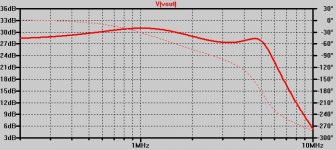
After checking the AC Analysis was received here such picture. In my opinion, the humps at 1 MHz and 4.5 MHz indicate possible problems with the stability that is critical. Therefore, it was decided to get rid of them - but this is impossible without loss of effective bands feedback. Your proposed correction was the only possible one. From my point of view, the use of a voltage amplifier stage with a common emitter leads to many problems with stability, forcing you to apply complex correction. In addition, were found the above-described possible problems with the stability of current regimes. Therefore, the study of your proposed circuit design was completed.
Unfortunately, the discussion about the characteristics of the circuitry do not contribute to the improvement of personal relationships, so please accept the assurances of respect for your work on the study of circuit design.
To receive some benefit from our intercourse try to investigate voltage amplifiers with output stage with a common base. You will appreciate their high performance with fewer transistors and easy correction of frequency response.
Attachments
Hi. Yes, you are absolutely right regarding the level of distortion.
I can in my defense to say: the chosen values of R46 and R47 5.6, R45 and R48 6.8 for greater depth of feedback will not be able to contribute to the stability of the currents of the transistors of the amplifier with changes of temperature and replacement of transistors.
Moreover, this does not help the current mirror Q1, Q2, Q29 and Q27, Q9 in 120W-TT-CFA-triple-TPOIC-efVAS-currmirror.asc. A small deviation (difference) of the currents from the mirror currents of Q3 and Q4 Q33, Q34 may not be compensated by feedback. So I brought the scheme into compliance with my views on stability of current regimes According to my notions, the resistance R46 and R47, R48 R45 needs to be several tens of ohms. And agreed on the current modes of controlled new mirrors with the modes of the transistors of the voltage amplifier.
I chose small value emitter resistor to keep distortion low, and I use CCS to keep the current stable. As I said in my opinion this amp does not get any better with active load (current mirrors) and I did not have thermal problem with current stability.
After checking the AC Analysis was received here such picture. In my opinion, the humps at 1 MHz and 4.5 MHz indicate possible problems with the stability that is critical. Therefore, it was decided to get rid of them - but this is impossible without loss of effective bands feedback. Your proposed correction was the only possible one. From my point of view, the use of a voltage amplifier stage with a common emitter leads to many problems with stability, forcing you to apply complex correction. In addition, were found the above-described possible problems with the stability of current regimes. Therefore, the study of your proposed circuit design was completed.
Unfortunately, the discussion about the characteristics of the circuitry do not contribute to the improvement of personal relationships, so please accept the assurances of respect for your work on the study of circuit design.
To receive some benefit from our intercourse try to investigate voltage amplifiers with output stage with a common base. You will appreciate their high performance with fewer transistors and easy correction of frequency response.
Why would our personal relationship suffer from some technical discussion? I don't have problem with technical criticism.
This amp was built in variants with VFET and BJT OPS and no problem with stability, I never built more stable power amp before.
Thank you for your time to analyze my amp, it always help to learn something more.
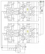
By the way, I have tried the balanced setup in simulator. The model is huge and rather slow - attached, just to show the "scale" of the "trouble" 😱
It utilizes 2 amp modules we already have and a tube phase splitter (came out pretty nicely). Simulated distortion levels are even slightly lower, than the ones for a single module.
And a lot of power. 600W no problem. Good setup for high-quality stage monoblocks. Can be easily equipped with XLR balanced inputs.
Preparing a tube splitter as a universal module now for convenient use with some other designs.
Cheers,
Valery
Attachments
For temperature stability of the cascade it is necessary that the voltage on the emitter resistors is much higher than the voltage of thermal noise (thermal voltage) 25 mV. That is, exceeded 250 mV. Or take other measures to stabilize the regimes of the cascade current. I did not find neither one nor the other.I chose small value emitter resistor to keep distortion low, and I use CCS to keep the current stable. As I said in my opinion this amp does not get any better with active load (current mirrors) and I did not have thermal problem with current stability.
Possible uncontrolled increase or decrease of the current of Q6 and Q8. I would pay special attention to this.
For temperature stability of the cascade it is necessary that the voltage on the emitter resistors is much higher than the voltage of thermal noise (thermal voltage) 25 mV. That is, exceeded 250 mV. Or take other measures to stabilize the regimes of the cascade current. I did not find neither one nor the other.
Possible uncontrolled increase or decrease of the current of Q6 and Q8. I would pay special attention to this.
Q3/Q11 and Q4/Q12 are thermally bonded, and Q11, Q12 current is controlled with CCS.
Last edited:
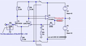
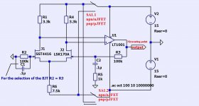
For semi-automatic selection of matched pairs of JFET and BJT. 🙂
The idea is that the OpAmp drove the J2 and balanced currents J1 and J2. In place of the J1 and J2 through connector placed a pair of JFET or BJT, and the output OpAmp to measure the voltage of the error and pick up a pair of JFET or BJT at the lower value.
For the selection of the BJT R2 = R3.
You can choose OpAmp any cheap device.
Attachments
It is possible to do so.
Attachments

Hi, I like to see your designs, I can see you have put a lot of thought into them, and perhaps some inspiration from Russian designs we haven't seen here.
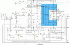
I'm worried that in your latest schematic, R33 may work against L6 and R50 for specific loads, although they're unlikely loads if you are only driving loudspeakers.
I'm worried that in your latest schematic, R33 may work against L6 and R50 for specific loads, although they're unlikely loads if you are only driving loudspeakers.
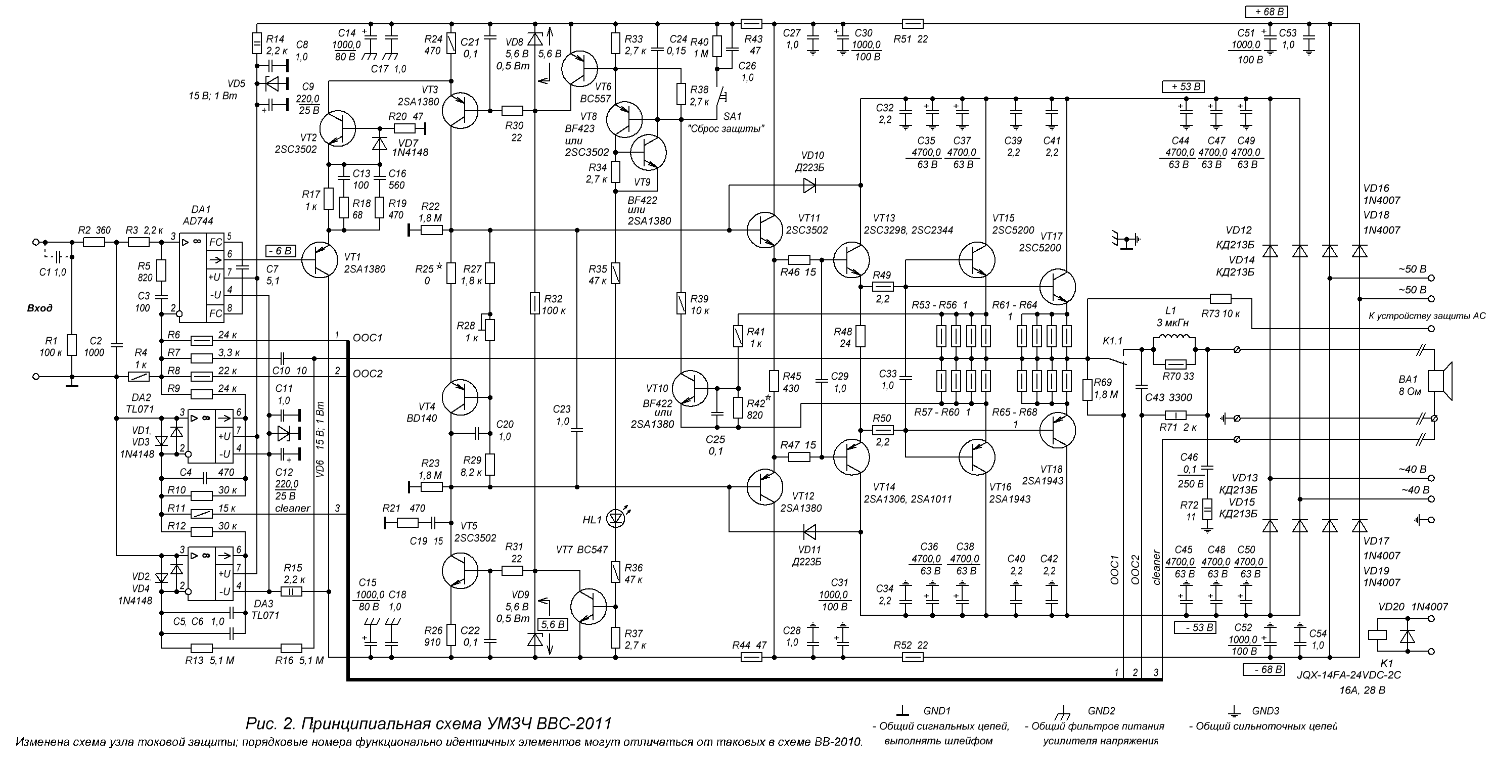
During the flow of distorted current is a low frequency loudspeaker of the speaker system on contact resistance of relay contacts, a speaker cable and coil of the output filter (the resistance of which is equal to the resistance of a few metres of speaker cable) to the connectors of the speaker system, we see the THD is 0.6% or more, and mount the IMD.
So you see how special negative feedback through R33C2 covered by the resistance of the output coil. R33C2 has a cutoff frequency above which the NFB does not work - to conserve the stability of the amplifier. This cut-off frequency far below the cutoff frequency of inductively coil and load capacity.
In addition, for the same purpose: to reduce the distortion from the distorted current of the low frequency loudspeaker from the speaker used several more knots and tricks, such as coverage of loop NFB of relay contacts and the use of special cascade compensation of the voltage drop across the speaker wires. They can be seen here:
http://www.diyaudio.com/forums/attachments/solid-state/548293d1462871663-several-schemes-2011.gif
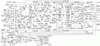
OpAmp DA2, which compensates the drop of a distorted voltage at the speaker cable amplification --2 times (R10/R11) is the voltage drop at the "cold" wire of the cable, and then feed the resulting voltage into the circuit using NFB R9 with the same resistance as the resistance in the circuit the NFB. At the output of the PowerAmp, you receive an incremental voltage equal to 2 the voltage drop at the "cold" wire that compensates for distortion from the speaker system, as it eliminates the cable altogether. In addition, it allows you to control your speaker system with high damping coefficients to avoid the effect of non-elastic, spongy bass.
In order to avoid the same: getting harmonics from the WOOFER to midrange speaker you have used connecting the speakers two cables, biwiring. This method is better than connecting the speakers through a single cable, but worse than the described method.
We see the coverage of the relay contacts circuit OOC1 (English: NFB1), which is valid until the relay connect speaker systems, and circuit OOC2 (English: NFB2) main NFB, which works after you connect this relay output PowAmp to the speakers.
Write in detail, considering the complexity and inaccuracy of machine translation.
Thank for Texas: I studied electronics on the book by experts from TI on designing amplifiers, televisions and radios. Of course, these people is no longer with us, but I thank them.
So you see how special negative feedback through R33C2 covered by the resistance of the output coil. R33C2 has a cutoff frequency above which the NFB does not work - to conserve the stability of the amplifier. This cut-off frequency far below the cutoff frequency of inductively coil and load capacity.
In addition, for the same purpose: to reduce the distortion from the distorted current of the low frequency loudspeaker from the speaker used several more knots and tricks, such as coverage of loop NFB of relay contacts and the use of special cascade compensation of the voltage drop across the speaker wires. They can be seen here:
http://www.diyaudio.com/forums/attachments/solid-state/548293d1462871663-several-schemes-2011.gif
OpAmp DA2, which compensates the drop of a distorted voltage at the speaker cable amplification --2 times (R10/R11) is the voltage drop at the "cold" wire of the cable, and then feed the resulting voltage into the circuit using NFB R9 with the same resistance as the resistance in the circuit the NFB. At the output of the PowerAmp, you receive an incremental voltage equal to 2 the voltage drop at the "cold" wire that compensates for distortion from the speaker system, as it eliminates the cable altogether. In addition, it allows you to control your speaker system with high damping coefficients to avoid the effect of non-elastic, spongy bass.
In order to avoid the same: getting harmonics from the WOOFER to midrange speaker you have used connecting the speakers two cables, biwiring. This method is better than connecting the speakers through a single cable, but worse than the described method.
We see the coverage of the relay contacts circuit OOC1 (English: NFB1), which is valid until the relay connect speaker systems, and circuit OOC2 (English: NFB2) main NFB, which works after you connect this relay output PowAmp to the speakers.
Write in detail, considering the complexity and inaccuracy of machine translation.
Thank for Texas: I studied electronics on the book by experts from TI on designing amplifiers, televisions and radios. Of course, these people is no longer with us, but I thank them.
Last edited:
Thanks for the explanation. I think I understand how it works, just not sure that it works in all cases.
His work depends on your views. 🙂 If you love the Warm Tube Sound, or the First Watt prefer the Second and Tenth, it doesn't work. 🙂
In all other cases, one OpAmp, three resistor, and so improve the sound in the bass, that in Russia, this node is set to PA since 1989. But to us he was from Japan, from the amplifiers "Toshiba" - "Clean Drive Sistem", "Kenwood" - "Sigma Drive Sistem", and "Akai" - "Zero Drive Sistem". Since this is a standard node in our amplifiers.
In any case, it need to test practically.
The first amplifier circuit refers to 1989, the second in 2001, third - 1999.
Attachments
Last edited:
His work depends on your views. 🙂 If you love the Warm Tube Sound, or the First Watt prefer the Second and Tenth, it doesn't work. 🙂
In all other cases, one OpAmp, three resistor, and so improve the sound in the bass, that in Russia, this node is set to PA since 1989. But to us he was from Japan, from the amplifiers "Toshiba" - "Clean Drive Sistem", "Kenwood" - "Sigma Drive Sistem", and "Akai" - "Zero Drive Sistem". Since this is a standard node in our amplifiers.
In any case, it need to test practically.
If I may... "node" = "circuit" above. Automatic translation artifact 😛
Thank you, just as I suspected. In our language the node is not the connection of the two wires, but functional unit.If I may... "node" = "circuit" above. Automatic translation artifact 😛
Last edited:
There is a problem with your punctuation.Distortion is below 0,000.4% 20 kHz 40 V / 8 Ohms failed to achieve.
Maybe that makes it clearer:
Failed to get level Distortion is below 0,000.4% 20 kHz 40 V / 8 Ohms.
"," is used as a decimal separator in European notation, while "." does nthe same in UK/USA notation .
You are using *both* in the same number 🙄 which of course is meaningless.
It was an accident. Indeed, in LTSpice IV, I have seen hundreds of times this punctuation.
There is another error. Actually achievable to reduce the level of measured (no sims) distortion of about 0.000,15%, and 0.000.3% in the most difficult case (20 kHz, output power at the threshold limit of voltage) can be obtained quite easily for amplifiers shown in some diagrams.
There is another error. Actually achievable to reduce the level of measured (no sims) distortion of about 0.000,15%, and 0.000.3% in the most difficult case (20 kHz, output power at the threshold limit of voltage) can be obtained quite easily for amplifiers shown in some diagrams.
Last edited:
- Status
- Not open for further replies.
- Home
- Amplifiers
- Solid State
- Several schemes