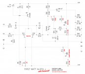
I spent this weekend adapting my first ever layout in KiCad of Aleph J to Alep J with 2 output transistors. I called this ver. Aleph Jazz. 😀 But that is not final.
I am still experimenting with symbols and so on.
Components have old numeration. Will fix that later.
Wow, nice work! Looks great!
I spent this weekend adapting my first ever layout in KiCad of Aleph J to Alep J with 2 output transistors. I called this ver. Aleph Jazz. 😀 But that is not final.
I am still experimenting with symbols and so on.
Components have old numeration. Will fix that later.
Nice! I like the sax 🙂
I spent this weekend adapting my first ever layout in KiCad of Aleph J to Alep J with 2 output transistors. I called this ver. Aleph Jazz. 😀 But that is not final.
I am still experimenting with symbols and so on.
Components have old numeration. Will fix that later.
Wow beautiful!

I spent this weekend adapting my first ever layout in KiCad of Aleph J to Alep J with 2 output transistors.
Uhm, I see two power transistors. I guess one is for the Aleph current source, and the other is the output. So where is the second output transistor?
Thank you for the feedback!
Thank you for suggestion Zen Mod!
Not everywhere possible with curent layout but I will try.
V inputs will require a bit of movement to double their traces.
Those was meant for Jupiter 600V 1uF copper foil cap but now there are places for Wima and so on caps with lead spaces: 15mm, 22.5mm, 27.5mm, and 37.5mm
I was meant two big output stage transistors. Sorry for confusion. 😱
wherever you can , double power traces to both layers
Thank you for suggestion Zen Mod!
Not everywhere possible with curent layout but I will try.
V inputs will require a bit of movement to double their traces.
Wow! Those big places for C1 seems perfect for my beloved russian PIOs 😀
Those was meant for Jupiter 600V 1uF copper foil cap but now there are places for Wima and so on caps with lead spaces: 15mm, 22.5mm, 27.5mm, and 37.5mm
Uhm, I see two power transistors. I guess one is for the Aleph current source, and the other is the output. So where is the second output transistor?
I was meant two big output stage transistors. Sorry for confusion. 😱
wherever you can , double power traces to both layers
I have found that's not usually possible with KiCad, it tends to automatically delete the other layer.
I use the 'Mask back' and 'Mask front' layers to create areas that can be built up with either a thick layer of solder, or solder on a length of 14 AWG tinned copper wire.
then use other program, which gives you more control
I can draw Gioconda on pcb in Eagle if I want ( ignore am I capable or not)
but, do not ask how much I paid my Eagle and where
🙂
I can draw Gioconda on pcb in Eagle if I want ( ignore am I capable or not)
but, do not ask how much I paid my Eagle and where
🙂
I have found that's not usually possible with KiCad, it tends to automatically delete the other layer.
I use the 'Mask back' and 'Mask front' layers to create areas that can be built up with either a thick layer of solder, or solder on a length of 14 AWG tinned copper wire.
There is a default setting to automatically delete redundant traces in KiCad. Uncheck that setting and you can put the same trace front and back.
From google: In Route menu check for Interactive routing settings. Uncheck “Remove Redundant Tracks” option
Last edited:
There is a default setting to automatically delete redundant traces in KiCad. Uncheck that setting and you can put the same trace front and back.
From google: In Route menu check for Interactive routing settings. Uncheck “Remove Redundant Tracks” option
I was wondering how you did what you did for the Singing Bush CRC boards you laid out in KiCad. At least I think that must be how you did it. Still at earliest stages of learning.

I can draw Gioconda on pcb in Eagle if I want...
🙂
I think that would be an excellent addition to the revised version of Aleph J for the SS device...
I will await that new board prior to starting.
maybe 6L6 is having something for you Greedy Boyz, regarding that...... if you ask him politely


Hi Cody,
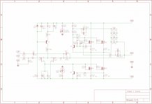
As I mentioned a few posts back, I'm planning to duplicate this with the Semisouths. I've been looking over your schematic and comparing to the Aleph J boards I have from the store. My first blush was that you just eliminated Q3, Q6, and Q8 and associated resistors, but that doesn't seem to be correct assumption.
Is it fair to assume that you had to do some jumpering to make your schematic from Post 81 work with the boards? For example, no connection between R16 and R4, nor from R11 to Q7 drain. I haven't done a complete check of the schematic to see if there are more changes. Any traces cut? Other jumpers?
I've attached the schematic for the original and your final revised schematic.
Thanks.
Attachments
Hi Cody,
As I mentioned a few posts back, I'm planning to duplicate this with the Semisouths. I've been looking over your schematic and comparing to the Aleph J boards I have from the store. My first blush was that you just eliminated Q3, Q6, and Q8 and associated resistors, but that doesn't seem to be correct assumption.
Is it fair to assume that you had to do some jumpering to make your schematic from Post 81 work with the boards? For example, no connection between R16 and R4, nor from R11 to Q7 drain. I haven't done a complete check of the schematic to see if there are more changes. Any traces cut? Other jumpers?
I've attached the schematic for the original and your final revised schematic.
Thanks.
So, there are some discrepancies between Nelson’s schematic and the schematic used to create the store boards. I used the FW schematic to mark-up, but the actual circuit I used would be the first schematic you attached. I believe the published FW schematic that I used has a couple of errors (which you caught.)
Regarding the removal of Q3 and associated resistors - that is completely optional, and something I did mainly to allow for experimentation. That said, this is the current limiting portion of the circuit and - depending on the source resistance and Iq you use - could activate prematurely. ZM should correct me if I’m wrong, but it’s activation depends on sensing the voltage drop across the output source resistor. I recall the standard bias recommendation saw a 400mV drop across the .47 resistor. If one keeps the same source resistance and goes down to a single device (as opposed to dissipating across parallel devices), you’d be looking at a 800mV drop - enough to activate the current limiter. For instance, I started out with .33R ohm source resistors and saw current limiting take effect (not that I could hear it).
For me it came down to two options (as I wanted to keep the Iq around 1A7):
- remove limiting circuitry
- alter source resistance so limiting circuit doesn’t trigger
Honestly, I don’t mind rolling the dice and removing the limiter parts. Others may prefer to leave it. No right answer IMO
Thanks for the fast response. If I understand, you removed the following:
Q6; R10; R17
Q8; R12; R19
and current limiting Q3; R13; R14
Several values changed and they are clearly marked on the revised schematic. But no jumpers added and no traces cut. If this is correct it makes more sense to me and very easy to make work. I followed the discussion of removing R18 and adjusting R24.
Thanks.
Yes, those are the exact changes I made. Other values I specified (mainly the source resistors) were more a representation of what I was aiming for, and what sounded good to me. I certainly can’t guarantee they weren’t detrimental to some other measurable aspect of the amp’s performance. After all, I’m a complete novice with a sound card, REW, and too much spare time - my words on these matters should carry no real weight 😀
Pa did remove it in J2
as I explained in PM - do not alter values in Aleph CCS, while you can play with source resistor of SS , somewhat altering OLG thus THD Spectra, in some way and measure
as I explained in PM - do not alter values in Aleph CCS, while you can play with source resistor of SS , somewhat altering OLG thus THD Spectra, in some way and measure
- Home
- Amplifiers
- Pass Labs
- Semisouth Aleph J?