I have seen this (a darlington) used by Rod elliot (esp) http://sound.westhost.com/project117.htm , on his project 117. But you say a very high beta device (such as a 2sc3503 - highest gain group Hfe 600+) would suffice ?? what device
would you suggest??
OS
I used KSC3503, with Hfe 300. It was good, but now the KSC2690A with Hfe 250 works better.
Sajti
Would you be referring to just the Vbe or the whole stage ??I meant to say CFP
Show me , LO. (pix)
OS
If you want to go more complex than one transistor rather use the complementary transistor multiplier then, better than the cfp.
Darlington transitor or very high Vbe transistor works well enough with triples like this, heres one I use for very high power amps, 400 watts up, 2sd1953.
Darlington transitor or very high Vbe transistor works well enough with triples like this, heres one I use for very high power amps, 400 watts up, 2sd1953.
Last edited:
I used complementary Vbe multiplier as well. With KSC3503/KSA1381. It was overcompensated, with triple darlington, so I decided to use the single transistor version.
Sajti
Sajti
homemodder,
manufactured Darlington transistors perform poorly. The CFP should be considered superior in all aspects.
manufactured Darlington transistors perform poorly. The CFP should be considered superior in all aspects.
Best way I have found to aliviate this little unfortunate problem is to use a very high beta vbe multiplier transistor or even better a darlington.
I'm not sure we are talking about the same thing. While I agree that it is desirable to have a stable bias spreader (perhaps using a high-beta Vbe multiplier or CFP Vbe multiplier) the problem I was referring to is the base resistance in the pre-driver, driver and output transistors of a Triple (especially the latter).
The DC voltage drop across the transistor's RB plus that across its base stopper can introduce temperature-dependent and device-matching dependent errors into the biasing. This can be especially so in regard to current hogging among paralleled output transistors.
Cheers,
Bob
(Attachment 2) is the total current required of the drivers by 5 pair 0281/0302's (double that for the NJW21193/4's) and the CCS currents (+- 22ma). All looks good. A strange refinement occurred to me ... since the P/N devices ,while close,are not perfectly matched. This makes the crossover points slightly different (from N to P - 58ma... back from P to N 64ma , just for example.) This effect seems to happen at frequencies over 10Khz and never at 1K.
Could this be the differences in Cob/beta between the P - N devices ?? By trimming one of the driver CCS's I found I could "lock" the Xover points within a mV independent of load or freq.
(attachment 3) This is Ib of the predrivers. With 2R loads small "glitches" occur that are perfectly in phase with the Xover points . What are they??? 😕
Any finally , the INSANE wire melting load (attachment 4) that still gives me
between .002% and .005% THD20. This holds true with either of my favorite OP's (NJW21193/4 or NJW0281/0302) , 2 - 8 R loads , and any # of OP pairs. Some might think me "thick" for wanting to keep the CCS's , but the FFT tells me to keep them as just about all the higher order harmonics are greatly reduced or eliminated.
OS
This is normal, as the driver are in class AB the cut off is inevitable, are not properly crossover distortion, not are axis zero if driver are in class AB shifts the distortion.
The higher the frequency and higher current worse is the effect, the junction can not off in time less than the frequency.
In your third graph, I noticed that the current Ib the TRs PNP is greater than the TRs NPN do not know what the reason.
-Difference of HFE between PNP and NPN think it should not be!
The basic cause for the impedance transform (one can look at it in either way, base-->emitter or emitter-->base) is the drop of hfe vs frequency. The critical region starts right at the point were this roll-off kicks in, if you have a transistor with hfe=100 and Ft=30MHz this point would be on the order of 300kHz, assuming a 20dB/decade rolloff.
This impedance transform is usually covered in modern textbooks in all detail.
Net links to a 3-part article by Dennis L.Feucht
http://www.analogzone.com/col_1017.pdf
http://www.analogzone.com/col_1121.pdf
http://www.analogzone.com/col_0116.pdf
- Klaus
Thanks for the links, Klaus.
HiI will try some of your suggestions. FYI I am using 100 ohms on the pre-driver bases. I have to admit I have nobase stppers on the output devices. I use a stanars zobel (0.1 uF 400vac cap and a 3 watt low inductance resistor. I am using a 1uH L for the output inductor. The zobel is on the amplifier side of the output inductor. Just to confirm, the amp is perfectly stable until I remove the 1nf caps from the driver bases to ground.
Bonsai
You are limiting the Slew-Rate with this capacitor in drive base to ground. I already had this problem, as greater is the bias, greater is the oscillation.
My problem was not in triple output, but in Miller compensation (this problem is not related to phase margin), I do not know what topology you use, I use VAS balanced, the output does not oscillate even at high frequency (1,5Mhz -3dB) I tested with different TRs.
The inductor at the output is for prevent oscillation with capacitive load.
Last edited:
Hi
You are limiting the Slew-Rate with this capacitor in drive base to ground. I already had this problem, as greater is the bias, greater is the oscillation.
My problem was not in triple output, but in Miller compensation (this problem is not related to phase margin), I do not know what topology you use, I use VAS balanced, the output does not oscillate even at high frequency (1,5Mhz -3dB) I tested with different TRs.
The inductor at the output is for prevent oscillation with capacitive load.
The C from the bases of the drivers to GND adds a pole in the amplifers output stagethat I want to get rif off. I quoted the above to fully describe the operating environment. I know about the output inductor and zobel.
I use a fully balanced VAS as well with Cascode.
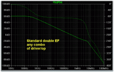
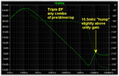
A possible "trouble with triples"
Very odd , A direct comparison of the open loop gain between a type 2 double EF and the new triple show certain things that are of concern (maybe).
While I do not totally trust in EXACTLY what the simulation shows , the differences between my known OPS (attachment 1) and the triple (attachment 2) merits further investigation. While I could get the triple to oscillate by omitting basestoppers or using super high gain drivers , as it is , it will do a square wave with no ringing and it is superior in the THD vs load department.
the 10.5mhz "bump" (attachment 2) concerns me. Same amp - different OP , another oddity ... even with the lower Ft OP's (njw21193/4 - 4mhz) , I do not understand how that can happen. 😕
I have tried different basestopper values , reverting to the standard "T" stage (no CCS's) , even using different voltage stages and compensations. I am confused ???
OS
Attachments
ostripper,
already the double Darlington means significantly increased distortions compared to a single transistor, as a price of higher current gain. No simulation is needed to substantiate that.
already the double Darlington means significantly increased distortions compared to a single transistor, as a price of higher current gain. No simulation is needed to substantiate that.
In think you guys are worrying too much with sims, build the circuit and you might be pleasantly surprised that it acts much diffrently than your sims.
My current triple I use on a super low THD circuit using mosfet outputs shows oscilations galore in sims but in real it is as tame as a baby puppy. Plz dont say its the models, they are the same everyone uses and I have some which have been developed by the application engineers of the manufacturer and much more accurate than the usual ones you get from the net.
Build prototypes and put a scope on it, then youll know for sure whats happening.
By home modder-In think you guys are worrying too much with sims, build the circuit and you might be pleasantly surprised that it acts much diffrently than your sims.
I totally agree , I am now running (attachment 1), and it sounds beautiful. No oscillation, no problems. I also"fixed" the loop gain aberration (attachment 2), with careful selection of the basestopper values.
With those same values the type 3 triple is just as "tame".. 🙂 I have to build it to really see.
OS
Attachments
Hi Ostripper,
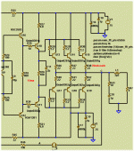
If I were you, I would try to decrease R27 and R31 to 1ohm and put 1uF from driver collector to ground 😉
Cheers,
Mihai
If I were you, I would try to decrease R27 and R31 to 1ohm and put 1uF from driver collector to ground 😉
Cheers,
Mihai
I totally agree , I am now running (attachment 1), and it sounds beautiful. No oscillation, no problems. I also"fixed" the loop gain aberration (attachment 2), with careful selection of the basestopper values.
With those same values the type 3 triple is just as "tame".. 🙂 I have to build it to really see.
OS
I use almost same triple darlington output, with same type of predrivers and drivers. The predrivers are running with 10mA, the drivers are runnning with 80mA, and the output is four pairs of FJL4215/4315, with 10ohm base stoppers. I found no oscillation. The base stoppers are soldered directly to the base of the transistors, with maximum 5mm long terminals
Sajti
- Home
- Amplifiers
- Solid State
- Self type 3 EF (hybrid triple)... any pointers ??