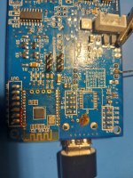
I have 39 ohm on output to 74ac157 and from 74ac157 also to dac.No pullup is needed. AK4121 outputs should probably have small physical size, roughly 33-ohm resistor in series (see attached image). The resistors should be located very close to the AK4121 output pins. What is coming out is RF so care needs to be taken to route it accordingly.
The 50-ohm transmission line in the image (sort of looks like a 50-ohm coax), is another thing to understand. https://www.allaboutcircuits.com/te...-life-rf-signals/what-is-a-transmission-line/
I saw, how look scope with/without this 39ohm, better with.
Now i have some problems with hardware, so now i need make some modification, i had to pull this chip up..
Attachments
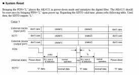
According pdf, i make reset, about 5ms reset signal to PND.
Still no data,clock and lrclosk in output..:/
master clock connected, 256 setup.
I still fight😉
Still no data,clock and lrclosk in output..:/
master clock connected, 256 setup.
I still fight😉
Attachments
Last edited:
Yes, sorry for qualityDo you have to scope to verify input signals are correct?
input signals correctly connected, mute to L, setup:
cmod0,1,2, L
odif 0,1 L
idef0 H
idef1 H
idef2 L
demo0 H
demo1 L
power 3,3V,
TVDD to 5V
Reset PDN 5ms
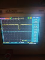
It is look like PLL not lock..output strange, all on L state, should be H...
Attachments

Last edited:
i looking for this...is clock should be 2,822,400MHz for 32 bits and 44.1K sample and not more?Do you have to scope to verify input signals are correct?
i connected 11M..it is to fast....
I setuped bypass-mode, works correctly
output work, so chip has problem with setup cmode.
on orginal radio, this chip working to convert LSB to i2s format...and works well, so why do not like to work in reverse mode?
setup in orginal radio:
demo0 - 1
demo1 - 0
de filter 48k
idef0 - 1
idef1 - 1
idef2 - 0
mod1 384 96k master
cmod0 - 0
cmod1 - 0
cmod2 - 0
idif 16 lsb r-justified
odif0 - 0
odif2 - 0
odif 20/16 i2s
Attachments
Last edited:
correct setup for original radio:
cmod0 - 1
cmod1 - 1
cmod2 - 0
256 divide
idif0 - 0
idif1 - 0
idif2 - 0
idif 16 lsb r-justified
odif0 - 1
odif2 - 0
odif 20/16 i2s
demo0 - 1
demo1 - 0
de filter 48k
data clock on orginal i 2.8224 Mhz, 44,1K 16bits
cmod0 - 1
cmod1 - 1
cmod2 - 0
256 divide
idif0 - 0
idif1 - 0
idif2 - 0
idif 16 lsb r-justified
odif0 - 1
odif2 - 0
odif 20/16 i2s
demo0 - 1
demo1 - 0
de filter 48k
data clock on orginal i 2.8224 Mhz, 44,1K 16bits
Last edited:
I2S clocks and data from the source device should be sent to AK4121 inputs. The 11MHz Master Clock is a separate signal that can be used as a frequency "reference" for the PLL (which tracks then incoming clocks to help convert the sample rate in the correct frequency ratio). Using a reference clock should assure that AK4121 output I2S signals will be synchronous with the dac clock. For that to work correctly the 11MHz MCLK signal needs to connect to AK4121, Pin-21. What you need to do is explained in AK4121 datasheet. Search for the term "MCLK" and read everything there is on it, would be my suggestion.
Last edited:
Nice, it was it!I2S clocks and data from the source device should be sent to AK4121 inputs. The 11MHz Master Clock is a separate signal that can be used as a frequency "reference" for the PLL (which tracks then incoming clocks to help convert the sample rate in the correct frequency ratio). Using a reference clock should assure that AK4121 output I2S signals will be synchronous with the dac clock. For that to work correctly the 11MHz MCLK signal needs to connect to AK4121, Pin-21. What you need to do is explained in AK4121 datasheet. Search for the term "MCLK" and read everything there is on it, would be my suggestion.
I connect mckl to 21 and now bt working well with cmod1,2,3 on L..now only find setup for rest mode and should working..
Divide 256 working ok for bt and 48K sample, for usb i have no data, but it can be setup problem .
Attachments
Ok i added reset 5ms and for one moment i can switch between BT (48k) to usb (44.1k) and i saw data..but i can not reproduced it..
It was look like zero data-> reset-> synchro-> normal data, but some reason it not work at 100%...i see lost LRclock when reset, but on datasheet is that reset can be done once after power on..so i cut power and connect to gpio (3,3v), disable power for 500ms, power on, after 300ms make reset for 5ms (second gpio) and put data to ak chip..
I have to investigate it a little bit more😉
Hmm, the same divide for usb and bt, bt ok, usb can not lock..strangeOk i added reset 5ms and for one moment i can switch between BT (48k) to usb (44.1k) and i saw data..but i can not reproduced it..
It was look like zero data-> reset-> synchro-> normal data, but some reason it not work at 100%...i see lost LRclock when reset, but on datasheet is that reset can be done once after power on..so i cut power and connect to gpio (3,3v), disable power for 500ms, power on, after 300ms make reset for 5ms (second gpio) and put data to ak chip..
I have to investigate it a little bit more😉
Maybe a good idea to check and make sure bt and usb clock frequencies are the same for BCLK and LRCK. Depending on the number of bits per word, BCLK may have to be different for a given LRCK.
Also, check to make sure bt and usb protocols are the same (I2S, RJ, LJ).
Also, check to make sure bt and usb protocols are the same (I2S, RJ, LJ).
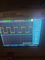
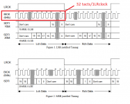
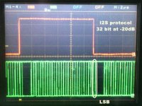
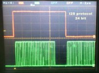
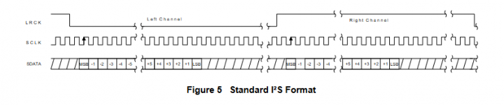
There is a way to see if you have I2S protocol, and how many bits there are, by using an oscilloscope. Using similar methods seems like it should be possible to identify LJ and RJ protocols. Some possibly useful pics attached I found on JL Sounds website, don't recall the exact link unfortunately. Top trace is LRCK, the frame clock. Lower trace is data at the bit clock rate. IIRC its what would be seen with a fixed-level sine-wave test signal.
Attachments

Last edited:
The first pic, bt.png, shows 32-bit words. The top trace appears to be LRCK (left/right clock). When LRCK is high there is the data for one channel, when LRCK is low there is the data for the other channel.
The bit clock, BCLK, shows 32 pulses per channel. All three pics look the same in that regard.
Now, the unanswered question is when in relation to LRCK edges does the data MSB start and the LSB end (for each source device). That's the difference between I2S, LJ, and RJ that we also want to take a look at. For that you will need to play a fixed level square wave, not music. Make a square wave at -20dBFS signal level, and another file with the signal level at 0dBFS. The -20dBFS file will make the more significant data bits all zeros. From that we can see which bit must be the LSB. Then we can see where the LSB is with respect to LRCK edges. The 0dBFS file will tell us how many data bits are actually in use by each source device. Also, we want to capture the bit patters when the square wave is at its peak level, not its edges. A LF square wave will have a longer dwell time at the peaks. We could try to use a rather LF sine wave instead, but we it might be harder to capture its bit pattern at the peaks, where we want to look. That's the idea anyway. Hopefully it will work.
To better understand, AK4121 datasheet, page 10 shows where the MSB to LSB data bits go with respect to LRCK edges. If those diagrams aren't clear I will attach an application note which goes into more detail.
Attachments
Last edited:
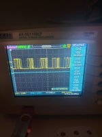
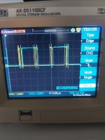
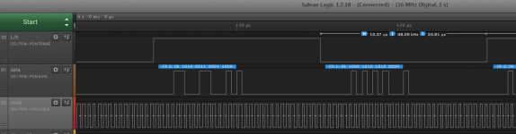
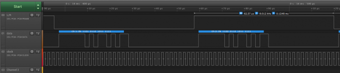
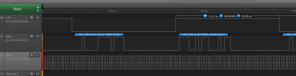
if it is i2s, should be like on screen.
ok i got it"
Therefore, the minimum required Serial Clock frequency is twice the audio sample rate
times the number of bits in each audio word"
so you have right, this is 32bit/channel
ok, i will try with sinus
ok i got it"
Therefore, the minimum required Serial Clock frequency is twice the audio sample rate
times the number of bits in each audio word"
so you have right, this is 32bit/channel
ok, i will try with sinus
Attachments
Last edited:
The signals are usually in two's complement notation, so for low-level signals with no DC offset, the MSB and the first few lower bits will all switch simultaneously in the same direction. With a square wave, depending on the exact level, the same may hold for the LSB and the first few bits above that. Maybe a -60 dBFS sine wave would be better, the highest ten bits then switch together while the lowest bits are either fixed at zero (when they are beyond the actual word length), or switch more or less irregularly.Now, the unanswered question is when in relation to LRCK edges does the data MSB start and the LSB end (for each source device). That's the difference between I2S, LJ, and RJ that we also want to take a look at. For that you will need to play a fixed level square wave, not music. Make the square wave at -20dBFS signal level, and another file with the signal level at 0dBFS. The -20dBFS file will make the more significant data bits all zeros. From that we can see which bit must be the LSB. Then we can see where the LSB is with respect to LRCK edges. The 0dBFS file will tell us how many data bits are actually in use by each source device.

https://www2.iis.fraunhofer.de/AAC/playpen.htmlThe signals are usually in two's complement notation, so for low-level signals with no DC offset, the MSB and the first few lower bits will all switch simultaneously in the same direction. With a square wave, depending on the exact level, the same may hold for the LSB and the first few bits above that. Maybe a -60 dBFS sine wave would be better, the highest ten bits then switch together while the lowest bits are either fixed at zero (when they are beyond the actual word length), or switch more or less irregularly.
maybe some of this file show more..
- Home
- Source & Line
- Digital Source
- sample conventer issue