OK! So below 1khz, all jitter from the s/pdif link is passed to the DAC 🙁
//
Not 1kHz, 1 Hertz.
An SPDIF link only creates high frequency jitter. Low frequency jitter comes from the oscillator in the source. The receiver chip PLL is only intended to get rid of link jitter, not source jitter.
An SPDIF link only creates high frequency jitter. Low frequency jitter comes from the oscillator in the source. The receiver chip PLL is only intended to get rid of link jitter, not source jitter.
Well, it will start to get rid of it above the PLL corner frequency... which can be 10 kHz like CS8416 (datasheet fig 25) or 1 Hz or something else, results will differ greatly...
Another question...on such board we have the fallowing outputs Optical (very high jitter) XLR , BNC and coaxial
What do you guys recommend as outputs..I think that coaxial + BNC is best.
What do you guys recommend as outputs..I think that coaxial + BNC is best.
Another question...on such board we have the fallowing outputs Optical (very high jitter) XLR , BNC and coaxial
What do you guys recommend as outputs..I think that coaxial + BNC is best.
The best overall choice for minimizing line reflection induced jitter is impedance matched unbalanced BNC. Blanced XLR and optical do, however, have an advantage in rejecting ground noise coupling between transport and DAC. Ground noise here might not only be audible in it's own right, but can increase noise induced jitter as well. That is especially true for optical.
Hi Ken
We wont use the Optical at all...since jitter is so high. Also our design will be galvanically isolated so I am not worried about ground noise. That leaves us with BCN and Coaxial
We wont use the Optical at all...since jitter is so high. Also our design will be galvanically isolated so I am not worried about ground noise. That leaves us with BCN and Coaxial
Peufeu, your imagination to create various simulation scenarios is great. I cannot even grasp how to simulate all these things you did.¨
I think we all agree that jitter is hard to get rid off in a "normal" fashion.
Personally, all music I'm listen to is via optical SPDIF ( from the TV and from my computer ). I really couldn't sleep well at nights realizing the crappyness of all these sources. So I decided to make a reclocking circuitry.
I have posted a brief description here on diyaudio before.
We here on diyaudio use to build things ourselves and perhaps that kind of technique may seem a bit complex, but it's not so very after all.
1. One Microchip DSP ( el cheapo )
2. A couple of counters, and gates. ( 74f168 x 2 and some nands )
3. One oscillator at 24.576Mhz ( this particular DSP has a max SR of 96khz due to speed limitations)
4. A bit C programming ( already done - including buffer adjustment techniques )
Now we only have to worry about our master clock which must be really stable. If you are interested I can give you schematics and source code.
I forgot to mention that this reclocker is located in my DAC ( or DAC's ). I have hooked it in to the I2S stream.
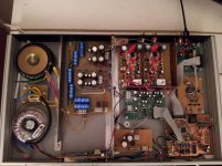
Look at my attached image. You see that gray flat cable? That's where the data normally is transferred from the receiver( CS8414) to the DAC ( pcm1704).
I cut it in two and inserted that messy thing to the bottom right which is an old prototype of an audio delay that didn't became anything.
Look at my attached image. You see that gray flat cable? That's where the data normally is transferred from the receiver( CS8414) to the DAC ( pcm1704).
I cut it in two and inserted that messy thing to the bottom right which is an old prototype of an audio delay that didn't became anything.
Attachments
Hi Ken
We wont use the Optical at all...since jitter is so high. Also our design will be galvanically isolated so I am not worried about ground noise. That leaves us with BCN and Coaxial
Hi, cdsgames,
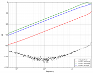
Transformers typically exhibit an decreasing CMRR as frequency increases, due to interwinding parasitic capacitance. Ground noise could still couple through this capacitance despite utilizing a transformer. While this is not an concern at power line frequencies it could cause problems in the presence of high frequency ground noise. Even so, high frequency ground noise might still produce audible artifacts via intermodulation.
Transformers also exhibit leakage inductance, which could disrupt the impedance matching of an otherwise impedance matched line. These two transformer design issues are counter to each other, improve one of them and the other gets worse. For example, reduce the leakage inductance and the parasitic capacitance increases.
OK, it has a SPDIF input which is decoded to I2S and the DSP receives this... what does the DSP do? Does it act as a FIFO to resynchronize incoming audio to a local master clock?
You are correct Ken , this is why I plan on isolating not the outputs...but the inputs.
Hi, cdsgames,
Transformers typically exhibit an decreasing CMRR as frequency increases, due to interwinding parasitic capacitance. Ground noise could still couple through this capacitance despite utilizing a transformer. While this is not an concern at power line frequencies it could cause problems in the presence of high frequency ground noise. Even so, high frequency ground noise might still produce audible artifacts via intermodulation.
Transformers also exhibit leakage inductance, which could disrupt the impedance matching of an otherwise impedance matched line. These two transformer design issues are counter to each other, improve one of them and the other gets worse. For example, reduce the leakage inductance and the parasitic capacitance increases.
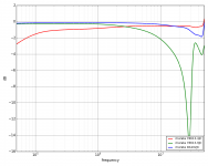
Here are 3 transformers, measured in transmission and common mode leakage using 50R network analyzer. In common mode they behave as capacitors, and isolation is inversely related to low end bandwidth extension... ie, smaller transformer = less low end and less capacitance.
Basically everything one would expect from theory 😀
Basically everything one would expect from theory 😀
Attachments
You are correct Ken , this is why I plan on isolating not the outputs...but the inputs.
I was referring to the input side of the interface.
Thats easy...LC filters on both input/output of transformer...ldos after.
I wasn't suggesting that these problems can't be mitigated, but rather that it requires awareness and engineering attention on the problem details to do so. The devil is always hiding in the details.
- Status
- Not open for further replies.
- Home
- Source & Line
- Digital Line Level
- S/PDIF and PLL