Please elaborate.
You wrote that there is no reason to see currents flowing between DAC and Sapphire by the signal ground, and that supplies are independent from each other. KVL/KCL equation set (for simplified layout as in your drawing) wouldn't preclude that in general. I guess those currents do exist in circuits, but effects of those are not necessarily audible; it depends on how impedances are defined for given components
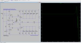
Compensation caps
Thanks. Out of curiosity, what was the peak frequency?
They are added to reduce the HF peaking observed in simulated frequency response.
So the answer is "for stability" though I have not noted any real-world instability and it is just as insurance. They can safely be left out.
Thanks. Out of curiosity, what was the peak frequency?
@mlackey
Around 40 MHz. Note that any amount of stray input capacitance will also damp that resonance out and the complete circuit bandwidth including the op amp (not shown) is far less, meaning the peak is already not so relevant, but adding the two 100 pF caps as shown settles it definitively.
@forta
Ah, Kirchhoff's equations. I wasn't familiar with the acronym, but I'm with you know. But no, I don't see how that enters into it. Currents originating from supply A can only return to supply A, and can only return to supply A through the common return wire to that power supply. There is no connection to Supply A through any of the supply B wires. To that extent they are independent, though they share a common reference.
Attachments
Compensation caps - final answer
I've learned something new today. Thank you!
@mlackey
Around 40 MHz. Note that any amount of stray input capacitance will also damp that resonance out and the complete circuit bandwidth including the op amp (not shown) is far less, meaning the peak is already not so relevant, but adding the two 100 pF caps as shown settles it definitively.
I've learned something new today. Thank you!
Hi there.
I am going to build the latest version of sapphire later in 2016.
So far the J-MO is running with my AKG 271 mk II pretty well.
I have been on the audio shop today and had listen to the basic Audeze model. They sounded interesting but the ifi amp driving them did not have enough drive for them obviously.
Wanted to check which headphones are you using with sapphire and does anyone has any experience with Audeze, are they giving a high load for an amp?
Sent from my ONE A2003 using Tapatalk
And another question.
There is a thread in vendors Vassar about the new TI amplifier
http://www.diyaudio.com/forums/showthread.php?p=4544074
Would this amp work with sapphire or is it too powerful for the headphones.
If it would what kind of adjustments would be required
Sent from my ONE A2003 using Tapatalk
There is a thread in vendors Vassar about the new TI amplifier
http://www.diyaudio.com/forums/showthread.php?p=4544074
Would this amp work with sapphire or is it too powerful for the headphones.
If it would what kind of adjustments would be required
Sent from my ONE A2003 using Tapatalk
Hi Oleg,
What you are asking for would require the following,
1. Circuit for the balanced->unbalanced conversion.
2. Circuit for the unbalanced->balanced conversion.
3. Four Sapphire amplifier boards.
4. Modification of headphones to use a four pin socket.
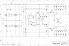
Parts 1,2 are generic audio design blocks and don't specifically relate to the Sapphire. You could could make your own, or I imagine they could be sourced from somewhere. An example circuit is attached, FYI.
rjm, I saw some photos of your amp housed in a casing similar to this one on Taobao.
https://item.taobao.com/item.htm?id=20846375865
Were you using the same casing?
For balanced, 4 PCBs are required? I see in your schematic that there are IN+, IN-, OUT+ and OUT- terminals on each PCB plus there are 2 transformers (1 per PCB)
Unless I'm missing something, isn't having 2 PCBs enough for balanced output with a 4 pole connector for the headphones?
And another question.
(TI OPA1622 Datasheet)
Would this amp work with sapphire or is it too powerful for the headphones.
If it would what kind of adjustments would be required
While it seems to have been designed specifically as a headphone driver, it is a high performance audio op amp and can therefore be used as the front end of the Sapphire circuit ... though not of course as a drop in replacement. It is a dual op amp, and comes in a truly minuscule surface mount package - and you'd need to wire up the GND and EN pins as well as the usual op amp connections.
rjm, I saw some photos of your amp housed in a casing similar to this one on Taobao.
https://item.taobao.com/item.htm?id=20846375865
Were you using the same casing?
That one is very similar, but I think it is smaller in all dimensions than the ones I used and does not have enough space to fit both PCBs and the power supply. There are lots of variants from Breeze audio and others.
You want one which is about 180 mm wide, like this one
for example given as 184x301x60mm (ebay link will expire).
For balanced, 4 PCBs are required? I see in your schematic that there are IN+, IN-, OUT+ and OUT- terminals on each PCB plus there are 2 transformers (1 per PCB)
Unless I'm missing something, isn't having 2 PCBs enough for balanced output with a 4 pole connector for the headphones?
OUT- is common (ground), not a negative driven phase. You can of course use a 4 pole connector for the headphones with just one board per channel, but it wont be balanced unless you drive both halves symmetrically, using two boards per channel with a phase splitter in front.
rjm, I saw some photos of your amp housed in a casing similar to this one on Taobao.
https://item.taobao.com/item.htm?id=20846375865
Were you using the same casing?
For balanced, 4 PCBs are required? I see in your schematic that there are IN+, IN-, OUT+ and OUT- terminals on each PCB plus there are 2 transformers (1 per PCB)
Unless I'm missing something, isn't having 2 PCBs enough for balanced output with a 4 pole connector for the headphones?
This one should be enough for two boards and trafos.
I am planning to use it.
it is actually the shop which sells chassis directly from the plant and quite efficient so far.
They are doing precision drilling and other customization by request.
Last edited:
That's the one for the chip amp LM3886 circuit and similar, so there is no headphone socket drilled in the front panel, an unwanted set of RCA cutouts in the back, and vents that you don't really want either.
The same case as the ebay one can be found on aliexpress (naturally), for example here.
The same case as the ebay one can be found on aliexpress (naturally), for example here.
I drilled it myself and asked to redrill later on. The guy is doing drilling based on your schematics
So no real need to stick to the design on the picture
We are getting a nice selection of different options now)

Sent from my ONE A2003 using Tapatalk
So no real need to stick to the design on the picture
We are getting a nice selection of different options now)
Sent from my ONE A2003 using Tapatalk
Last edited:
Bench notes:
Now that my Sapphire has well and truly settled down, and my new Rike PIO caps have arrived, it is a good time to try a few couple of things from the to-do list.
Today, I tried removing C2 and C3 from the boards.
What this is supposed to do: improve PSRR some 10 dB or so below 2-3 kHz, at the expense of re-introducing some 40 MHz peaking the caps were there to damp out, all according to the simulation.
What is seems to actually do: sound becomes slightly brassier, more intense, with enhanced rhythmic drive. Maybe a bit too much of a edge now?
Verdict: inconclusive. Pretty subtle either way. Worth trying if you think the Sapphire is slightly on the dull side ... but be careful, the caps break into two halves quite easily.
Last edited:
DC Voltage question
Completed my build over the weekend. A "quick look" looks very good: hf square waves are square, frequency response is flat, and DC offset very low. Much more promising than others I've tried.
I am measuring 7.9V DC on the outputs (emitters) of the pass transistors, Q11 and Q12. This seems low. I see 15V on the collectors (from bench supply), but around 8.6V on the base (where 8.6V minus a 0.7V diode drop = 7.9V). Both boards are within, say, 5% of one another, so I have to conclude it's by design.
Maybe it's because R23-R25 (and R24-R26) form a voltage divider between collector and base? I'm guessing here. A quick explanation would be greatly appreciated. I'm learning as I go.
Today, I tried removing C2 and C3 from the boards.
FWIW, I tried a similar change on a completely different board (hifisonic small signal class a), and heard a difference, but in the opposite direction. The original used a 50pf compensation cap in the feedback loop. I increased the cap to 100pf as an experiment. It did change the overall sound, less bite and a bit more laid back. The changes were subtle but my ears heard a difference. To me at least, it makes sense that removing the cap in the Sapphire would subtly change the sound. That may be something I play with in the future.
@mlackey
Double-check you drop 12V across the Zeners D1 D2. This will put 12 V onto the base of the transistors Q11 Q12, less the voltage drop across R25 R26 which is supposed to be about 0.5 V. The voltage between the emitters and COM/GND, i.e. V+ V- at the op amp, should be 10.6 V or something in that vicinity.
There is a remote possibility you got 10 V Zeners by mistake. If the Zener is 12 V and the transistor base is 8.6 V it means the circuit is drawing more current than it is supposed to, causing a greater voltage drop in R25 R26.
You can double check bias current by measuring the voltage drop across R19, R20 and applying Ohms Law. About 30 mA is expected, generating 30-35 mV drop across the 1 ohm resistors R19 and R20.
Attachments
Last edited:
Good guess!
RJM,
You are correct. Measured 8.8V across the zeners, snipped them out, checked the (very small) part numbers, they're (1N)4739 parts, 9.1V zeners. Everything else measures out just fine. 3.7mA across R7-R8, 38mA across R19-R20, a few hundred microamps across R11-R12.
No clue how those got in there. Probably one of the Southpark gnomes.
But even with the 9V parts, it sounds great. I'm very impressed with the DC offset: around 1mV on one board and less than that on the other. The biggest problem I have now is to find the 12V zeners. I know they are here somewhere.
Thanks for your patience.
There is a remote possibility you got 10 V Zeners by mistake.
RJM,
You are correct. Measured 8.8V across the zeners, snipped them out, checked the (very small) part numbers, they're (1N)4739 parts, 9.1V zeners. Everything else measures out just fine. 3.7mA across R7-R8, 38mA across R19-R20, a few hundred microamps across R11-R12.
No clue how those got in there. Probably one of the Southpark gnomes.
But even with the 9V parts, it sounds great. I'm very impressed with the DC offset: around 1mV on one board and less than that on the other. The biggest problem I have now is to find the 12V zeners. I know they are here somewhere.
Thanks for your patience.
Good, that was relatively painless troubleshooting. 38 mA through R19.20 tells me everything else it ticking over just fine.
The difference in Zener voltage is not critical, but 12 V is nominally the optimal value to use.
The difference in Zener voltage is not critical, but 12 V is nominally the optimal value to use.
- Home
- Amplifiers
- Headphone Systems
- RJM Audio Sapphire Desktop Headphone Amplifier