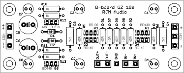
To check a few things, I'm building a second set with an experimental BOM, BOMX below.
- Emitter resistors R3,4 lowered to 1k to increase the bias current.
- Emitter resistors R7,8 lowered to 1R, which raises the bias current in the output stage to more closely match the driver stage, at the expense of stability and increased likelihood of thermal runaway.
- Ceramic bypass caps added in parallel to the four electrolytics after the Z-reg. If there is any high frequency stability issues, this should quiet things down.
Hi RJM
Any follow up in your experiment for items 1 and 2 when you lowered the resistor value?
What is the effect on the sound ?
thanks
kp93300
Hi RJM
One more thing .
Have you compered the sound difference with buffer build with BC and BD transistor?
Which is more transparent ?
thanks again
kp93300
One more thing .
Have you compered the sound difference with buffer build with BC and BD transistor?
Which is more transparent ?
thanks again
kp93300
@dimkasta
For the input resistor use whatever you have it's just a non-critical part, with no power draw.
@kp93300
Most of the changes came from the ceramic bypass caps. Changing the resistor values didn't make much difference, or at least not enough for me to get a handle on. All things considered, I should probably update the BOM values to the BOMX values. The extra current doesn't cost much from a design perspective.
I haven't played around with alternate transistors, of course just about anything can be used if you want to experiment...
questions from electronic illiterate
Hi Richard,
i am going to build this buffer with BD devices and compare to B1 from NP.
I am using it as a line level buffer after the LDR volume control and there is an output caps in the dac before the LDR
Hope you can clarify a few points for a electronic illiterate like me.
1)What is the current draw?
2)What is the dc voltage range usable for the buffer? My transformer is 18 0 and 18 0 ac.
3) If i use +/- 24 V dc before the Z reg, do i need a 1W zener in stead of 1/2 w ?
4) Will help it in lowering power supply noise by using LED for voltage regulation in place of zener?
5) Are the values of the cap critical?
6)How to match the transistor to get lowest dc offset ? What are the variables that determine the dc offset?
thanks for sharing your project
kp93300
i am going to build this buffer with BD devices and compare to B1 from NP.
That should be interesting. Just remember to have the ceramic bypass caps installed before you run off and start making comparisons.
1)What is the current draw?
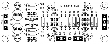
Kit BOM runs at about 12 mA per channel.
2)What is the dc voltage range usable for the buffer?
Kit BOM has 25 V capacitors. That's your upper limit. 18 VAC secondaries will blow the caps, but if you are dead set and you are sourcing your own parts anyway the BOM can be changed to operate at considerably higher voltages. I can provide the modified BOM. Email me.
3) If i use +/- 24 V dc before the Z reg, do i need a 1W zener in stead of 1/2 w ?
No, the Zener is running near its minimum current. Even with 24 V V++ the power dissipation does not increase significantly.
4) Will help it in lowering power supply noise by using LED for voltage regulation in place of zener?
I can't imagine it would be worth the trouble. R12, C7 are very effective at filtering out the Zener noise.
5) Are the values of the cap critical?
No, not at all. You can move a factor of 2 either way.
6)How to match the transistor to get lowest dc offset ? What are the variables that determine the dc offset?
I'm not sure as I haven't tried. I would assume matching hfe would do the trick. What you really want for low offset though is identical Vbe for a given static current and temperature.
Last edited:
In the buffered VSPS/Phonoclone scenario, if we ommit the Z-reg parts, where do we connect the common X-reg psu output? On the power pads on the buffer side?
Oh and have you noticed a difference connecting the buffer before (replacing R6/R8) and after the coupling cap (C3) ?
Dimitri
Oh and have you noticed a difference connecting the buffer before (replacing R6/R8) and after the coupling cap (C3) ?
Dimitri
Haven't tried the latter, I've only had the B-board after the phonoclone C3.
For the former, and I admit I hadn't considered it before you asked, V+ and V- connect back to the B-board from the Phonoclone, but on the B-board neither the COM not the GND need be connected to anything. The common path is already made by the phonoclone's OUT-. In principle... I may be mistaken; you'll have to feel it out as you go along.
For the former, and I admit I hadn't considered it before you asked, V+ and V- connect back to the B-board from the Phonoclone, but on the B-board neither the COM not the GND need be connected to anything. The common path is already made by the phonoclone's OUT-. In principle... I may be mistaken; you'll have to feel it out as you go along.
About BOMX, any comments on the increased bias changes?
Have you decided to make this the standard bom?
I am asking because you mentioned some possible instabilities and thermal drifting.
Have you decided to make this the standard bom?
I am asking because you mentioned some possible instabilities and thermal drifting.
Yes, from now on I will use the BOM with R3,4 1k and R7,8 1R. This is, as much as anything, to lower the number of different resistor values. I don't think it changes the sound much if at all. The board layout has also been revised to add the bypass caps C1A-4A.
Attachments
OK cool.
Just received the 100nF caps by the way 🙂
It s been almost a week since I have assebled the boards, but work is pwning me badly so I didn t test them yet.
For the time being I don t think I have the energy to test them both with and without the 100nF caps.
We ll see...
Just received the 100nF caps by the way 🙂
It s been almost a week since I have assebled the boards, but work is pwning me badly so I didn t test them yet.
For the time being I don t think I have the energy to test them both with and without the 100nF caps.
We ll see...
Hi Richard
I blew the Q5 and 6 during testing last night .
This morning i realize that I have not place insulation when i tie the back of Q2/3 and q1/4.
I have created a short from V- to V+!!!. The back of this transistors are connected to the collector !!
I have already replace Q5 and Q6 in the cap multiplier and power output tested Ok at + 11.9 and -12V dc.
Is there any likelihood of damage to Q1 to Q4??
regards
kp93300
@dimkasta
It can be a bit of a pain if you can't access the underside of the boards easily. I understand. Please report at least the sound with the caps in when you get the chance.
@kp93300
What transistors were you using? BOM calls for BD135,136, which are isolated TO-126, ECB pinout. Fortunately, transistors are cheap. I suspect Q5,6 blew out before the other transistors were damaged. Your voltages are normal, so I'd say you are OK. If you are using metal-backed transistors, you'll need an isolation pad between the back-to-back transistors. BCE packages will end up with the "back" facing out, which wont work very well but is probably OK for the B-board since the currents are so low, thermal feedback gained by stacking them together is probably not needed.
By the way it's a regulator, nor a capacitance multiplier. The zener diodes provides an absolute voltage reference.
Last edited:
Hi Richard
After placing insulation between Q 1 to Q4, the buffer works !
the dc offset remains at a stable 0.4 V without the 100K across the input. With the 100K at the input between the +ve signal input and ground, it is a stable 0.15V.
I have a cap in the amp input and the buffer is placed after the Lightspeed clone volume control.
The bd139 abd bd140 in the regulator runs a few degree above ambient temperature.
Q1 to Q4 has no detectable change in temperature.
I will post my view of the sound after running in.
I removed the ceramic bypass cap in the power supply after initial testing and the rather pronounced ssssss in vocal region.
I will put it back to test after more run in of the caps .
Do i need to run the signal through it for burning in process?
thanks to richard
regards
kp93300
No, just leave it powered up for a couple of days.
0.15 V is normal for 100k across the inputs. Was 0.4 V measured with the lightspeed connected?
0.15 V is normal for 100k across the inputs. Was 0.4 V measured with the lightspeed connected?
THe 0.4 v dc offset is measured when it was not connected to the lightspeed.
The pronounced sssss is traced to the input caps that is raw. i removed it and the see through and hear through perception is improved.
regards
kp93300
The pronounced sssss is traced to the input caps that is raw. i removed it and the see through and hear through perception is improved.
regards
kp93300
BTW, will changing the Q5 and Q6 in the power supply regulator to a darlington such as TIP 121 and 126 work ?
My build is bread board and easy to change.
kp93300
My build is bread board and easy to change.
kp93300
I don't think there is a lot of point* to switch to darlington, but it should certainly work. The output voltage is lowered by 0.6 V as there are now two diode drops between reference and output.
* I haven't simulated it, but I suspect there is no improvement in the output ripple, which is already low, and the noise produced by the darlington and injected into the output may likely by higher than a single transistor as a result of the higher gain.
* I haven't simulated it, but I suspect there is no improvement in the output ripple, which is already low, and the noise produced by the darlington and injected into the output may likely by higher than a single transistor as a result of the higher gain.
- Status
- Not open for further replies.
- Home
- Source & Line
- Analog Line Level
- RJM Audio B-Board Project