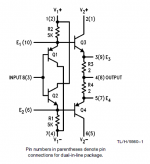
I've been into buffers lately. Diamond buffer, from the LH0002 datasheet (and the related app note), and, a more recent find, a variant from the TI document "Current Feedback Op Amp Applications Circuit Guide" which has a few more damping resistors**. They are really versatile circuit blocks. Line driver, unity gain preamp, preamp output stage, headphone amp output stage...
So I'm going to try and develop a circuit board or two, the founding idea being "small, cheap, simple, easily available, reliable." This is the sketchpad thread, I'll post the changes as they come... don't expect anything in final form.
Right now I've got three distinct variants in mind, depending on whether you want to drive 10k line impedances (low current version, TO-92, no thermal feedback), headphones (high current version, TO-126, heatsinks) and with or without voltage regulation.
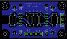
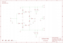
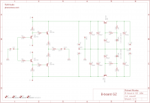
First up is the the most basic: low current version, no regulation. The "B Board Mini". 4x7cm board. I'm thinking people can retrofit this into their VSPS and Phonoclone projects - or anything at all, really. You are looking at the pre-alpha version below, not even worth posting the eagle files yet.
**These extra resistors are nice because they naturally give you a few more jumpers to work with, greatly simplifying the board layout.
So I'm going to try and develop a circuit board or two, the founding idea being "small, cheap, simple, easily available, reliable." This is the sketchpad thread, I'll post the changes as they come... don't expect anything in final form.
Right now I've got three distinct variants in mind, depending on whether you want to drive 10k line impedances (low current version, TO-92, no thermal feedback), headphones (high current version, TO-126, heatsinks) and with or without voltage regulation.
First up is the the most basic: low current version, no regulation. The "B Board Mini". 4x7cm board. I'm thinking people can retrofit this into their VSPS and Phonoclone projects - or anything at all, really. You are looking at the pre-alpha version below, not even worth posting the eagle files yet.
**These extra resistors are nice because they naturally give you a few more jumpers to work with, greatly simplifying the board layout.
Attachments
Last edited:
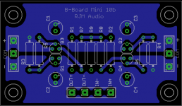
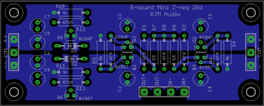
B-Board mini rev 10b
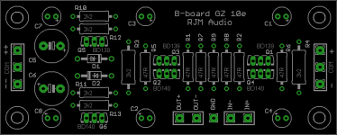
Finished the unregulated version of the buffer board, though I will later "metricize" the final board dimensions and hole spacing.
- using TO-92/SOT-54 EBC transistor packages, BC547/557 shown but any similar can be used
- extra set of redundant power supply connections, so boards can be daisy chained or rotated 180 degrees and the supply wiring stays neat
- Q1/3 Q2/4 back-to-back so the transistors can be glued together for thermal feedback
These boards are designed to run from a regulated, split +/- 9-12 V supply.
Dual sided boards 4x7 cm.
Attachments
Self-regulated, with Z-reg
"And for my next trick", said the Magician, waving his magic wand...
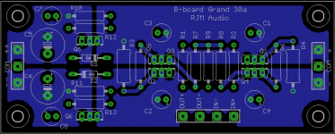
With the last board, we had the line-driver buffer circuit powered by a regulated supply. What we have here is the same buffer but for use with an unregulated power supplt. It has an on-board voltage regulator made up of a Zener reference and series pass transistors (a circuit block I have just dubbed the "Z-reg".)
This is the smallest version, with TO-92 packages. It's 4x10 cm, or half the size lengthwise of the Phonoclone 3 - or 1/4 Eurocard I believe. It's designed as a bolt-on upgrade for the Phonoclone, VSPS, any line level source components, phono stages, DACs, etc. It could also be used as the output stage of a pre-amplifier.
The regulated voltage is available from the pads on the right side, to power an external op amp voltage amplifier stage. As long as the circuit doesn't need much more than 10 mA... i.e. it's an op amp or two. As such there are all sorts of uses.
Next up, to see if we can replace the TO-92 with TO-126 type packages and some small heatsinks without increasing the board size all that much. If so we have a headphone buffer, the ultimate drop in upgrade for a chu-moy.
"And for my next trick", said the Magician, waving his magic wand...
With the last board, we had the line-driver buffer circuit powered by a regulated supply. What we have here is the same buffer but for use with an unregulated power supplt. It has an on-board voltage regulator made up of a Zener reference and series pass transistors (a circuit block I have just dubbed the "Z-reg".)
This is the smallest version, with TO-92 packages. It's 4x10 cm, or half the size lengthwise of the Phonoclone 3 - or 1/4 Eurocard I believe. It's designed as a bolt-on upgrade for the Phonoclone, VSPS, any line level source components, phono stages, DACs, etc. It could also be used as the output stage of a pre-amplifier.
The regulated voltage is available from the pads on the right side, to power an external op amp voltage amplifier stage. As long as the circuit doesn't need much more than 10 mA... i.e. it's an op amp or two. As such there are all sorts of uses.
Next up, to see if we can replace the TO-92 with TO-126 type packages and some small heatsinks without increasing the board size all that much. If so we have a headphone buffer, the ultimate drop in upgrade for a chu-moy.
Attachments

Last edited:
Well, that was easier than expected...
Now we have 1000uF filter caps, 2W "411” resistors R3, R4, and TO-126 ECB transistors (BD135,BD136 or equivalent). Heatsinks can be used, the clip on or screw on types have clearance underneath for the resistors.
This can either be a headphone buffer or a line buffer, depending on the value of resistors R3, R4 which set the bias current in the diamond buffer.
Attachments
Last edited:
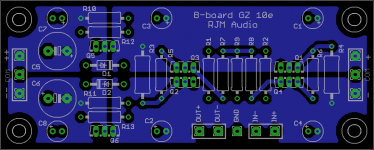
B-board GZ 10e
For those following along, the boards ("GZ" [Grand, Z-reg] variant, rev "10e") are now "RTM" status. I should get the first batch in a couple of weeks, then I'll have a look though and do some evaluation to fine tune the BOM values.
Also putting together a project page, here.
For those following along, the boards ("GZ" [Grand, Z-reg] variant, rev "10e") are now "RTM" status. I should get the first batch in a couple of weeks, then I'll have a look though and do some evaluation to fine tune the BOM values.
Also putting together a project page, here.
Attachments
Last edited:
A nice, clean, purpose built pcb would be nice as opposed to the perfboard I use.
These would come in handy for expeimenting with diamond, or other buffers/output circuits.
Let us know when you get the boards.
These would come in handy for expeimenting with diamond, or other buffers/output circuits.
Let us know when you get the boards.
Sure thing. I expect to start shipping by the end of Feb.
I'm glad you see things the same way I do re. having a PCB. Though I would say the B-board is multi-purpose built rather than purpose built. It's a go-anywhere, do-anything kind of board.
I'm glad you see things the same way I do re. having a PCB. Though I would say the B-board is multi-purpose built rather than purpose built. It's a go-anywhere, do-anything kind of board.
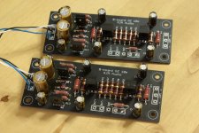
A photo of the finished boards.
The Q1/4 and Q2/3 are glued together for good thermal contact.
Notice In+ and In- are tied together with a resistor across the input. This required for testing, as the B-board expects to be attached to an input load normally.
Regulator output V+/- are 11 V and -11 V. Output offset voltage about 50 mV in both channels. 2 mA bias current in both output stages.
Everything working according to plan.
Attachments
B-board application note
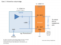
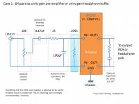
Is it is hard to write instructions that say "do this" or "do that" when so many different configurations are possible.
Shown in the attachments are the basic use cases as I see them. Either the B-board is going to be the "front end" in the chassis, accepting the line input signal directly, or it is going to be a traditional buffer, bolted on to the back of another circuit in the chassis.
Both cases are covered, I hope.
Any questions, please ask.
Attachments
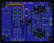
Hi Richard ,just connected today- B boards to VSPS300i
V++ and V-- measures 35V, Dc off set measures 150mV and 240mV for L and R chanels respectively( same for in/out off set).
Is that too high?
Quan
V++ and V-- measures 35V, Dc off set measures 150mV and 240mV for L and R chanels respectively( same for in/out off set).
Is that too high?
Quan
@quan
Unless you have a DC-coupled amplifier, this offset, while slightly on the high side, is OK.
The VSPS output has an coupling capacitor, C3, so the DC impedance seen from the B-board input is high, equal to R7 or 75k.
If you connected a smaller resistor across the B-board inputs from IN+ to IN-, perhaps 10k, you would see the offset voltages very much reduced (<50 mV). Actually I'd recommend you do that if you can. Exact value isn't critical, roughly 10k to 22k.
The other option is a little more complicated: move C3 and R7 to the other side of the B-board. This is done by inserting the B-board in place of R6 (VSPS) or R8 (Phonoclone). The resistor is removed from the board, the inputs go to the pad connecting to the op amp output, the outputs to the pad connected to C3. See attached.
Richard
Attachments
Last edited:
@quan
Unless you have a DC-coupled amplifier, this offset, while slightly on the high side, is OK.
The VSPS output has an coupling capacitor, C3, so the DC impedance seen from the B-board input is high, equal to R7 or 75k.
If you connected a smaller resistor across the B-board inputs from IN+ to IN-, perhaps 10k, you would see the offset voltages very much reduced (<50 mV). Actually I'd recommend you do that if you can. Exact value isn't critical, roughly 10k to 22k.
The other option is a little more complicated: move C3 and R7 to the other side of the B-board. This is done by inserting the B-board in place of R6 (VSPS) or R8 (Phonoclone). The resistor is removed from the board, the inputs go to the pad connecting to the op amp output, the outputs to the pad connected to C3. See attached.
Richard
Will do Richard
Insert 10K resistors. New DC offsets- 39/45mV respectively.
Beautiful music at moment.
Initial impression- more air and lower noise floor level.
Thank you Richard.
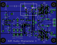
BTW- do you think the resistor will be needed for the PC3 as well?
Quan
Beautiful music at moment.
Initial impression- more air and lower noise floor level.
Thank you Richard.
BTW- do you think the resistor will be needed for the PC3 as well?
Quan
I'm very glad to hear it's working now.
The short answer is "yes": 10k resistors across IN+ and IN- can be used for both phono stages to reduce the offset voltage.
It's the way the B-board circuit operates: the output offset is a function of the DC impedance (resistance) seen between IN+ and IN-.
If there is a blocking capacitor upstream, the B-board cannot "see" the low impedance output of the driving stage, and instead has to source/sink current from the resistor placed between IN+ and IN-.
(Full disclosure - I forgot about the influence on output offset voltage of the blocking capacitor, basing the performance instead on the Sapphire amp, where the buffer is driven directly by an op amp and the total output offset voltage is extremely low, less than 10 mV.)
Both the Phonoclone and VSPS normally have this blocking capacitor, so the output offset depends on whatever resistors to ground are placed after the blocking capacitor (C3). This is normally 75k for my phono stages. That's - a bit marginal. 10k is better, if only for peace of mind.
Last edited:
Richard,
If one inserts the buffer in the Phonoclone circuit in place of R8, I assume that a 75k or less resistor needs to be added across the input of the buffer also, since the buffer no longer sees the phonoclone 75k at its input?
Martin
If one inserts the buffer in the Phonoclone circuit in place of R8, I assume that a 75k or less resistor needs to be added across the input of the buffer also, since the buffer no longer sees the phonoclone 75k at its input?
Martin
No, that's not needed. When the circuit is powered, the buffer input sees the op amp output impedance of IC2 (phonoclone) on its inputs, this is basically 0 ohms. There is also a convoluted DC resistance to ground through the feedback resistor R6.
Buffer installed (for the time being after the coupling cap of the Phonoclone). Works perfectly, about 160mV offset on one channel and 180 on the other without adding additional resistors on the input.
Verdict - very positive. With the Phonoclone I had been swapping out the 2nd opamp between the OPA27 and AD797 baing unsure which I prefered. The OPA27 was more mellow and listenable for a long session, but the AD797 seemed to carry a little more weight as well as detail and resolution, but at the expense of a certain edginess, that despite adding power pin decoupling never went away.
Now with the buffer added, the OPA27 setup gains the detail and weight of the AD797, without the edginess. I am sure that the easier driving of the buffer for the OPA27 is the reason, plus the buffers immunity to what it is driving.
I can thoroughly recommend the buffer!
I'll post pictures of the completed set up in a few days, the wiring is messy at the moment due to the addition of the buffers.
- Status
- Not open for further replies.
- Home
- Source & Line
- Analog Line Level
- RJM Audio B-Board Project