Now boys and girls...this is getting interesting.
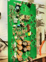
I have populated one board. except for the outputs, big caps, fuses and the dual JFET.
I found a transformer outputting a bit more than 30VAC and used a variac to power up the amp driver section and protection. I was hoping to hear the relay click.
Well, output had like 7VDC so I soldered a 100ohm resistor across it, now there is like 100mV = 1mA.
One thing is that a 4.7uF cap by the protection circuit was reversed on my board. I soldered it in like in the schematic posted here recently. I think it should be that way. - to GND?
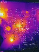
But yes. R34 gets very hot for me. Like 100deg.C (1.8k 4W) and with my thermal imager I could see that T12 and R13 get a bit warm, like 50deg.C.
Hmm...maybe I have to wait for the JFETs to arrive.
Feedback does not work without it 🙂
I have populated one board. except for the outputs, big caps, fuses and the dual JFET.
I found a transformer outputting a bit more than 30VAC and used a variac to power up the amp driver section and protection. I was hoping to hear the relay click.
Well, output had like 7VDC so I soldered a 100ohm resistor across it, now there is like 100mV = 1mA.
One thing is that a 4.7uF cap by the protection circuit was reversed on my board. I soldered it in like in the schematic posted here recently. I think it should be that way. - to GND?
But yes. R34 gets very hot for me. Like 100deg.C (1.8k 4W) and with my thermal imager I could see that T12 and R13 get a bit warm, like 50deg.C.
Hmm...maybe I have to wait for the JFETs to arrive.
Feedback does not work without it 🙂
Attachments
Good news ! I am waiting for my output MOSFET's to arrive yet.
After that I will be testing.
I will assemble everything except output and protection. I think that it is better to test the amp without the last. Once I am sure that it is reasonably stable, I will complete the protection.
After that I will be testing.
I will assemble everything except output and protection. I think that it is better to test the amp without the last. Once I am sure that it is reasonably stable, I will complete the protection.
You are right. Totally unnecessary to have the protection circuit there now.
But easily bypassed. I guess it is delay & DC prot?
Or is it something else too?
Any views on C105 4.7uF? In your first post it is positive to GND as on my PCB.
In the later schematic it is the other way.
It has a small voltage that is of the right polarity when + goes to GND.
But it is like 100mV, so I guess it is much higher in some situation.
Maybe if my driver voltage was correct then relay would energize or something... 🙂
I will try to return to this end of next week.
Hi all,
I think this thread died. Or does someone have any news?
I could still do some attempts to get it working.
I listed my project for sale, I have about 30 amp projects so some will have to go 🙁
I even have the transformers if someone is interested 🙂
Thanks anyway to everyone who tried to help and I hope my comments have been of some use 🙂
Hi all,
I think this thread died. Or does someone have any news?
I could still do some attempts to get it working.
I listed my project for sale, I have about 30 amp projects so some will have to go 🙁
I even have the transformers if someone is interested 🙂
Thanks anyway to everyone who tried to help and I hope my comments have been of some use 🙂
No! It's not dead!
I am doing this😉
Attachments

Posiadam 2x3 pary 2sk133 2sj48 w starej niemieckiej studyjnej końcówce mocy (150 RMS na kanał/8R, stabilna w 2,5R). Czy są dobre do zbudowania tego wzmacniacza.
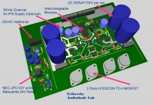
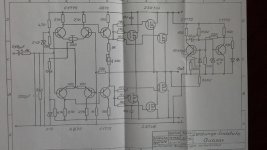
On The Photo is a circuit diagram of my power amplifier (one channel without protection board).
On The Photo is a circuit diagram of my power amplifier (one channel without protection board).
Attachments
I have 2x3 pairs 2sk133 2SJ48 in an old German studio power output (150 RMS per channel/8r, stable at 2.5R). Are they good to build this amplifier.
On The Photo is a circuit diagram of my power amplifier (one channel without protection board).
English please.
dave

diyAudio moderation team
I was writing in English. It's idiotic Google translator do translation to my language like all post. Writing in English isn't problem for me.English please.
dave
diyAudio moderation team
I don't have it because i don't need it.
Hello
What are the best alternative for BSS71 and BSS74?
These 200V transistors are not easy to find (with heatsink) !
Thanks for help!
What are the best alternative for BSS71 and BSS74?
These 200V transistors are not easy to find (with heatsink) !
Thanks for help!
https://www.nxp.com/docs/en/product-change-notice/PCN3763.txtHello
What are the best alternative for BSS71 and BSS74?
These 200V transistors are not easy to find (with heatsink) !
Thanks for help!
Not sure if best options, but worth a try.
https://www.onsemi.com/pdf/datasheet/mpsa42-d.pdf
https://www.onsemi.com/pdf/datasheet/mpsa92-d.pdf
https://www.onsemi.com/pdf/datasheet/mpsa42-d.pdf
https://www.onsemi.com/pdf/datasheet/mpsa92-d.pdf
Hi! Could you start a private conversation with me? Your private is inaccessible.KatieandDad please are you talking about the PCB layout of post #1 ?
Alex mm , did you designed this PCB of post #1 ?
I would like to kindly ask everybody to stick to the original model of 2 power output MOSFET's , because this is the reason why this thread was started. Please be so kind to read the #1 post. The idea is to put order for those who have this PCB model, despite we can later get into details for changing it to a better version.
Thank you very much.
Last edited:
Hello team
I have some heat issue making my version of this amplifier with 4 max pairs of mosfet.
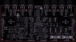
I am sharing the PCB files that the great Alex shared with me.
Here:

I would like to reduce the heat of T11, T12 wich are now MPSA 93, 43
and I would like feedback about my idea of reducing the value of R20.
I am doing some tests, powering up the circuit from 0 to -15V, +15V and
mosfets a becoming hot while the transistors that cannot be touched with your fingers...
Instead T9 seems to be the last to become operative with slow power up sequence.
Any feedback is appreciated. Best regards.
matteos
matteos
Thanks in advance
I have some heat issue making my version of this amplifier with 4 max pairs of mosfet.
I am sharing the PCB files that the great Alex shared with me.
Here:
I would like to reduce the heat of T11, T12 wich are now MPSA 93, 43
and I would like feedback about my idea of reducing the value of R20.
I am doing some tests, powering up the circuit from 0 to -15V, +15V and
mosfets a becoming hot while the transistors that cannot be touched with your fingers...
Instead T9 seems to be the last to become operative with slow power up sequence.
Any feedback is appreciated. Best regards.
matteos
matteos
Thanks in advance
Attachments
- Home
- Amplifiers
- Solid State
- Revision of Very Best Amplifier ... 2015