Please correct bias current next to the R22=330R.
There should be 10mA not 100mA. If Vgs of one buz900 will be approx 1.5V so we need around 3V across that resistor = 10mA.
On the other hand I do not know how MPSA42/92 are dissapating so much heat (60V*10mA=600mW, they will be very warm!!)
Regards
Peter
There should be 10mA not 100mA. If Vgs of one buz900 will be approx 1.5V so we need around 3V across that resistor = 10mA.
On the other hand I do not know how MPSA42/92 are dissapating so much heat (60V*10mA=600mW, they will be very warm!!)
Regards
Peter
Hello borys ! Thank you.
I will correct the note in the schematic. I have heard from the original thread that these transistors work very warm and that they need heat sinks.
By the way, have you build this amplifier before ?
I will correct the note in the schematic. I have heard from the original thread that these transistors work very warm and that they need heat sinks.
By the way, have you build this amplifier before ?
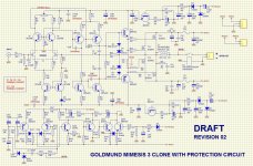
Problems on power supply
Dear all,
I am also busy building my own Mimesis3 clone. During commissioning of the power supply, I observed R27=10k as well as R32 is getting hot. After some measurements i get a little confused. The voltage over R27 is 84V. That means about 700mW Power disipation. I use Resistors of 0,125W Power class, which is far to small and will change them to 1W power class. The Voltage over C9 and C7 is also 84V but according the drawings, 63V Types are suggested. I don't know why they are not blown up yet 🙂. The Output voltage on T12 is 84V. The same results I got on the negetive path. Is this correct? Can somebody help me?
Tanks in advance
Rico
Hi,
the negative rail is not conected to ground. I use the same transformer configuration as posted at beginning of this thread. So all relevant parts like R27, C7-10, Diode are connected to the middle Point on tranformer.
the negative rail is not conected to ground. I use the same transformer configuration as posted at beginning of this thread. So all relevant parts like R27, C7-10, Diode are connected to the middle Point on tranformer.
Yes, I gather it's a source of controversy. Either way will work, just change the bias point slightly. Supposedly that's how it was in the original Goldmund, and if it isn't broken don't fix it?

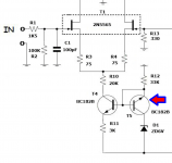
This little piece seems very unusual, especially since it is connected in series with a 6 volt Zener diode ....
_
BJT can be used reverse biased as a zener with voltage between 6 to 8 V, depends of bjt type.
If this transistor act as ordinary diode then the tail current is 2 mA, to low for 2N5565 with Idss between 5 and 30 mA.
There were originally schematics showing the BE junction used as if a zener, but I didn't keep track of why this schematic was settled on. If the clones have a lower Jfet bias, then they might be more stable than the original.
Is that clone PCB a copy of the original layout or was it designed from the available schematic?
Is that clone PCB a copy of the original layout or was it designed from the available schematic?
There were originally schematics showing the BE junction used as if a zener, but I didn't keep track of why this schematic was settled on. If the clones have a lower Jfet bias, then they might be more stable than the original.
Is that clone PCB a copy of the original layout or was it designed from the available schematic?
Maybe more stable, but with higher distortion as jfet is more linear close to its Idss.
As shown in Post #28 this particular BJT is operated in forward bias. Very unusually it is the base-to-collector junction that forward biased. Ptype base, Ntype collector. It smells like an error to me, especially since the BJT-diode is connected in series with a 6 volt zener diode.BJT can be used reverse biased as a zener with voltage between 6 to 8 V, depends of bjt type.
As shown in Post #28 this particular BJT is operated in forward bias. Very unusually it is the base-to-collector junction that forward biased. Ptype base, Ntype collector. It smells like an error to me, especially since the BJT-diode is connected in series with a 6 volt zener diode.
Tempco compensation?
Not really since the current is (Vbc + Vzener - Vbe)/Remitter.
If you want this current to have zero tempco (dI/dt = 0) then Vbc would magically have to track the weighted sum of the resitor's tempco, the zener's tempco, and the current source transistor's Vbe tempco. Since neither the zener nor the resistor are specific part# devices on the schematic, their tempcos are unknown AND their tempcos change from amplifier to amplifier as the purchasing department buys yet-cheaper parts from different distributors. So: no, it's not a tempco trick. It's just a design error.
If you want this current to have zero tempco (dI/dt = 0) then Vbc would magically have to track the weighted sum of the resitor's tempco, the zener's tempco, and the current source transistor's Vbe tempco. Since neither the zener nor the resistor are specific part# devices on the schematic, their tempcos are unknown AND their tempcos change from amplifier to amplifier as the purchasing department buys yet-cheaper parts from different distributors. So: no, it's not a tempco trick. It's just a design error.
It does seem a bit weird IMV.
If connected conventionally the LTP current is approx 2 mA. Connected as shown with the E-B junction Zenering' about double that.
If connected conventionally the LTP current is approx 2 mA. Connected as shown with the E-B junction Zenering' about double that.
Do you see that emitter is shorted to base?Connected as shown with the E-B junction Zenering' about double that.
Is that clone PCB a copy of the original layout or was it designed from the available schematic?
This is the original PCB, using star ground on top layer.
Attachments
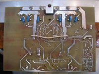
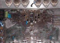
Thank you for posting that photo. It shows how the original Goldmund amplifier used a removable potted "module" which fit into the 24 pin DIP socket at center top.This is the original PCB, using star ground on top layer.
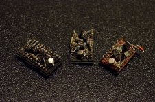
The "Goldmund Clone" PCB photo in post #30, seems to have unpacked the internals of the module and laid them out as discrete components on the board. Text says "Schematic: Nagysaudio" so I visited their website and found this photo which Nagys claims to show the internal details of Goldmund modules after decapsulation. Nagys claims to have reverse engineered the modules and are offering their versions for sale, to anyone who is repairing or refurbishing a Goldmund amplifier.
_
Attachments
- Home
- Amplifiers
- Solid State
- Revision of Very Best Amplifier ... 2015