Marcel,
Just wondering if you have seen the discrete dac implementation in Marantz SA-10 player? Schematics are in the publicly available service manual.
Interesting that per channel, they use no more than a 5.6 V Zener/avalanche diode, an NPN emitter follower and a couple of resistors and capacitors as the DAC reference regulator in an 8000 euro SACD player!
Would not be surprised if that sounds better than a textbook LT3042 reference for this particular application. The rest of output stage is also kind of interesting. Multiple discrete, but fairly unsophisticated op amps. The SA-10 is said to take a couple of hours to fully warm up to sound its best. Hoping to listen to one before too long and compare the sound to my Topping D90. Should be interesting 🙂
JRC's line of IC opamps are also fairly unsophisticated and, it seems extremely likely, so are their MUSES imprinted opamps which audiophiles praise and pay thru the nose to purchase.
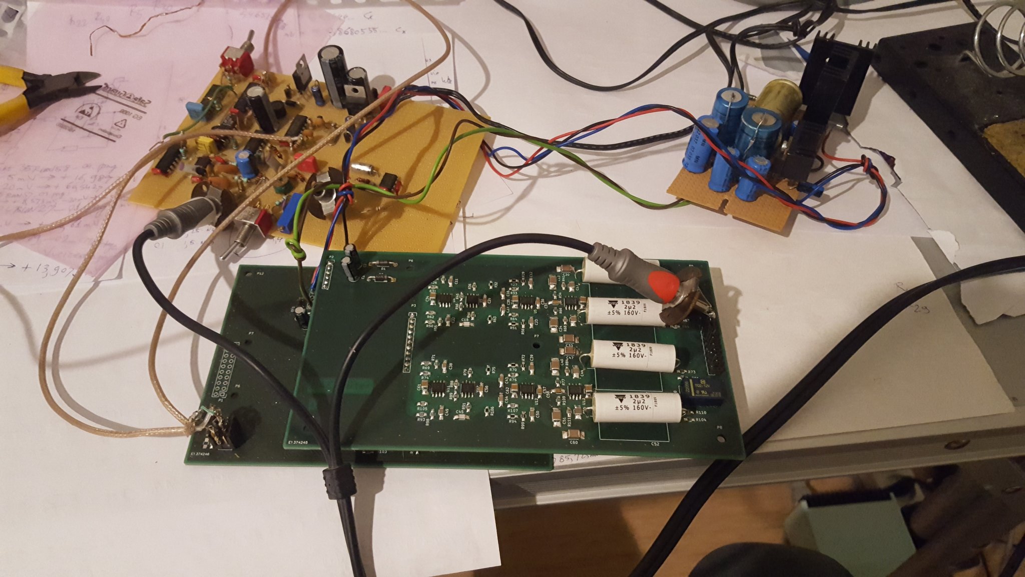
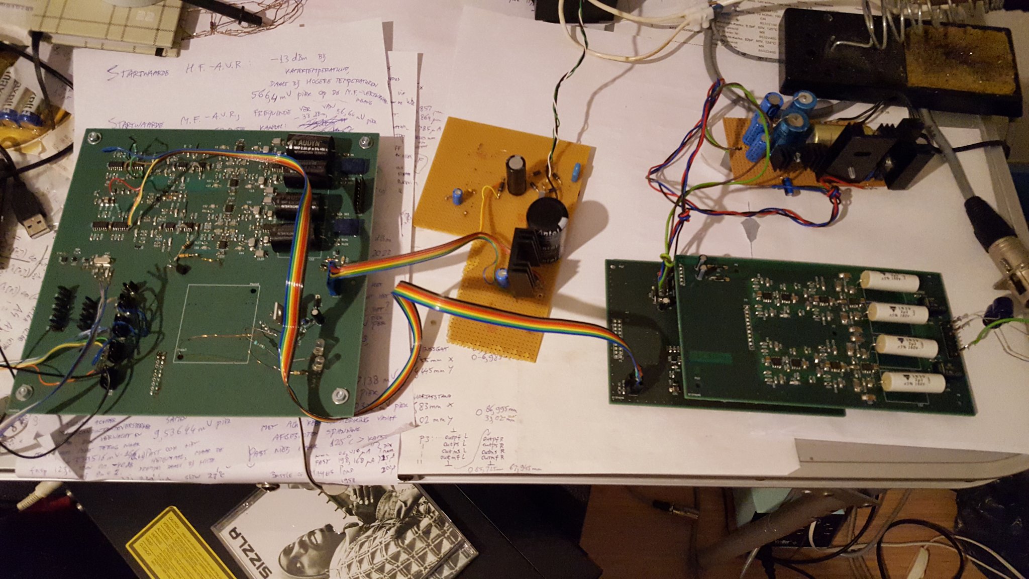
There is an analogue audio signal coming out of the DAC, out of the positive side of the left channel and the negative side of the right channel anyway (I haven't checked anything else yet). The biggest perfboard is a simple sigma-delta ADC I use for an analogue to digital to analogue test.

Last edited:
@MarcelvdG ,
It probably was covered somewhere already but I seem to have missed it.... what's the advantage of the RTZ concept over a conventional DSD FIR DAC like the one from Jussi (Signalyst)? I note Jussi's DAC uses a far longer sliding window.
It probably was covered somewhere already but I seem to have missed it.... what's the advantage of the RTZ concept over a conventional DSD FIR DAC like the one from Jussi (Signalyst)? I note Jussi's DAC uses a far longer sliding window.
Differences between the rising and the falling delay don't cause distortion with RTZ. Hence, they also don't cause audio noise due to intermodulation between ultrasonic quantization noise components.
Jussi's DAC will be less sensitive to far-off phase noise/period jitter than mine. That's due to the longer FIRDAC and the non return to zero method. With a return to zero DAC, you need twice the number of taps for a given (far-off) jitter sensitivity.
Jussi's DAC will be less sensitive to far-off phase noise/period jitter than mine. That's due to the longer FIRDAC and the non return to zero method. With a return to zero DAC, you need twice the number of taps for a given (far-off) jitter sensitivity.
Last edited:
Thanks for the explanation, understood.Differences between the rising and the falling delay don't cause distortion with RTZ. Hence, they also don't cause audio noise due to intermodulation between ultrasonic quantization noise components.
Jussi's DAC will be less sensitive to far-off phase noise/period jitter than mine. That's due to the longer FIRDAC and the non return to zero method. With a return to zero DAC, you need twice the number of taps for a given (far-off) jitter sensitivity.
I get the idea is to make all "1" (and "0", resp.) symbols 100% electrically identical (same energy) which is only the case when there is some defined blank space surrounding them. That space needs at least to be as long as the settling from the slopes will take, right? Doubling the clock frequency is a relative simple way to insert those blanks but actually it is not a requirement.
If that blank time is just as short as actually required this would increase SNR (by a larger output voltage for the same modulation level), wouldn't it? Say, if it's only like 10% of the clock period rather than the full 50% one would almost have non-RTZ levels and still have the benefits of RTZ.
It seems one could as well use gating at the shift register outputs (with AND-gates) and a proper gating signal that blanks, say, the first and last 1/8th segments of a symbol (generation of this gating from the clock, independent of clock frequency, is the hard part here).
I'm also gathering that in a balanced operation the blanks need to inserted after the polarity inversion otherwise there is a systematic DC offset, that's why inserting zeros in the source stream (in a converter to 2x the rate) rather than in hardware will not be fully succesful.
Exactly. On top of that, the load on the voltage reference has to be as data-pattern-independent as possible.
I made a logic gate DAC some time ago, see https://www.diyaudio.com/community/...th-97-db-a-dynamic-range.313520/#post-5214065 The present DAC is supposed to be an improvement on that (see post #166 of the linked thread), but whether it really is, is still to be determined.
I made a logic gate DAC some time ago, see https://www.diyaudio.com/community/...th-97-db-a-dynamic-range.313520/#post-5214065 The present DAC is supposed to be an improvement on that (see post #166 of the linked thread), but whether it really is, is still to be determined.
Last edited:
I hooked up the digital part of my earlier logic gate DAC to the shift register DAC to see if it works at 27 Mbit/s and if it has a lower noise floor.

The good news is that it works, the bad news that the A-weighted noise floor is 10 dB worse: -87 dB(A) with respect to the maximum sine wave level instead of -97 dB(A).
The good news is that it works, the bad news that the A-weighted noise floor is 10 dB worse: -87 dB(A) with respect to the maximum sine wave level instead of -97 dB(A).
I wanted to check if splitting the flatcable to separate the clock part from the data part would reduce data-to-clock crosstalk and lower the noise floor. It had practically no effect, but by chance I found out that moving the whole cable could substantially reduce the noise, to about -98.7 dB(A). I haven't a clue why yet. To be continued...
I only use gold plated connectors for clock signals. With regard to clock jitter, found out the hard way that tin can be very sensitive to weakening-with-time contact pressure and or little spots of corrosion. Don't know if that could be an issue here.
Thanks! The connectors are gold plated and brand new, but I'll keep poor contact in mind as a possible root cause anyway. I did use other tools than I should to attach the cable: a soldering iron and a miniature screwdriver instead of a special crimping tool.
I've had several bad experiences with those ribbon cables Marcel, both with the crimped connectors and poor continuity in the the cables - I now make up my own cables with good quality wire and I solder the connectors - I put a little solder paste into the connector before crimping them and then hold an iron on them.
almost the same experience with this connectors... 🙁
simply any tool is not enough, soldering is final.
.
@MarcelvdG maybe this cables are too long?
I have had several times just same situation when moving ribbon cable was changing the things.
What about the fround planes in these PCB-s. Is there some common power supply PCB module?
simply any tool is not enough, soldering is final.
.
@MarcelvdG maybe this cables are too long?
I have had several times just same situation when moving ribbon cable was changing the things.
What about the fround planes in these PCB-s. Is there some common power supply PCB module?
That could very well be the case. If it were an ideal transmission line, its length wouldn't matter as long as at least one side were perfectly terminated, but in reality neither the cable nor the termination is ideal. The power supply of the left PCB is completely separate from the supply of the right two PCBs. The grounds are connected via four of the seven flatcable wires.
I made the data cable much shorter, replaced the clock cable with a short, thin 75 ohm coax cable (RG-179) soldered on both sides, and tapped off the clock a bit earlier in the clock chain of the PCB that generates the clock and data signals. The noise floor now dropped to around -107 dB(A).
I need to measure it more accurately, because there is too little difference between the noise with the DAC off and with the DAC on. I subtract the noise power measured with the DAC off from the measured noise power when playing silence, but as there is only a 0.59 dB level difference, the result gets very sensitive to measuring inaccuracies.
I need to measure it more accurately, because there is too little difference between the noise with the DAC off and with the DAC on. I subtract the noise power measured with the DAC off from the measured noise power when playing silence, but as there is only a 0.59 dB level difference, the result gets very sensitive to measuring inaccuracies.
good news 🙂
IF the consumption is not a huge maybe to try the battery power suply?
Sometimes opening one end of sheild in coax cable could made a difference from my experience...
IF the consumption is not a huge maybe to try the battery power suply?
Sometimes opening one end of sheild in coax cable could made a difference from my experience...
- Home
- Source & Line
- Digital Line Level
- Return-to-zero shift register FIRDAC