TomWaits said:
He's a BIG Poobah and likes big bling around the neck.🙂
Thanks, but I should have no difficulty getting the transsitors. I'm not done yet with the substitutions so hold that thought.
I have decided to refurbish the orriginal output boards but what do you mean exactly by bulking up copper? Sounds interesting?
Shawn.
If I get the board b4 etching, when the copper is all one electrically connected piece, I can add copper by electroplating to whatever thickness you'd want. Only limit to thickness is undercutting when etching, as lateral etch can accelerate as depth increases. Or if you need individual traces repaired on the refurbed original, I can plate those too, limited only by lateral expansion bridging traces.
auplater said:If I get the board b4 etching, when the copper is all one electrically connected piece, I can add copper by electroplating to whatever thickness you'd want. Only limit to thickness is undercutting when etching, as lateral etch can accelerate as depth increases. Or if you need individual traces repaired on the refurbed original, I can plate those too, limited only by lateral expansion bridging traces.
So you CAN thicken an etched board but the traces may widen on the sides just as they do on the surface? Over plating would drive the traces into each other? Sorry for my crude words but I want to get a handle on it. Do I understand?
Plater, what exactly do you do for a living?
Cheers,
Shawn.

Hi. If the PCB images are available, I would like a copy. I own a very nice DC-300A too 😉
Thanks in advance...
SB
Thanks in advance...
SB
TIP558
The DC300A had a TIP558 TO-3 (or similar) mounted on the ouput board & heat sink. For each rail it was the last driver before the 2N5631 TO3 outputs.
TIP558 NPN TO-3
IC 7.5A
VCEO 250
HFE Min 6
HFE max -
IC 5A
VCE 2v
VCESAT 2.5v
VCESAT IcA 10A
PT 100Watts
What is the best option for this, or has it been mentioned already?
Shawn.
Attachments
Images
Shall we try emailing them? What resolution do you require to etch? 600dpi, 300dpi?
Email me and I will get them over to ya asap.
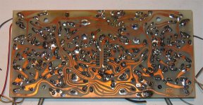
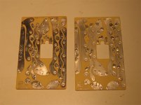
I will post all of this on the net when I'm done but perhaps I should get on that sooner? I did not use a professional PCB artwork program but I have been debating importing my images into a board layout program to gain full artwork and generate proper silk screens, even gerbers? This will take much time as I am still a newbie on PCB software. I scanned the actual printed cicuit boards with my scanner and then photo-shopped them. Very crude technique at best! Many hours but I enjoy it. 😉
Shawn.
Algar_emi said:Hi. If the PCB images are available, I would like a copy. I own a very nice DC-300A too 😉
Thanks in advance...
SB
Shall we try emailing them? What resolution do you require to etch? 600dpi, 300dpi?
Email me and I will get them over to ya asap.
I will post all of this on the net when I'm done but perhaps I should get on that sooner? I did not use a professional PCB artwork program but I have been debating importing my images into a board layout program to gain full artwork and generate proper silk screens, even gerbers? This will take much time as I am still a newbie on PCB software. I scanned the actual printed cicuit boards with my scanner and then photo-shopped them. Very crude technique at best! Many hours but I enjoy it. 😉
Shawn.
That's what I thought
Good Times!
Thanks,
Shawn.
anatech said:Hi Shawn,
Just use an output transistor for the TIP558.
-Chris
Good Times!
Thanks,
Shawn.
TomWaits said:
So you CAN thicken an etched board but the traces may widen on the sides just as they do on the surface? Over plating would drive the traces into each other? Sorry for my crude words but I want to get a handle on it. Do I understand?
Plater, what exactly do you do for a living?
Cheers,
Shawn.
basically yes... the metal doesn't know to only grow up....unless there's photoresist or some sort of barier to stop it. Lots of tricks though...
Currently I run a medical practice... but formerly worked in aerospace , private and government research labs, inkjet printing machine fabrication, built microwave waveguides for JPL, NASA/Goddard , EPA, NRAO, etc... plus private electroforming business...that sort of thing
John L.
auplater said:
basically yes... the metal doesn't know to only grow up....unless there's photoresist or some sort of barier to stop it. Lots of tricks though...
Currently I run a medical practice... but formerly worked in aerospace , private and government research labs, inkjet printing machine fabrication, built microwave waveguides for JPL, NASA/Goddard , EPA, NRAO, etc... plus private electroforming business...that sort of thing
John L.
So...if I give you...say 100 pounds of lead, you could...say turn it into GOLD? I see the pot in the avatar! You are an alchemist?
? You would be an amazing neighbor. 😀 Cheers,
Shawn.
re: nsd128 as far as im aware its a d44, i will get some pics on here of various transistors on the main boards, i currently have 11 dc300a's (dont laugh) 90% are original and all have various transistors fitted, basically no 2 are the same, because lets face it they made several thousand over a period of years i would have thought ........
d40 also crops up (these are available stateside surely?) no special devices, i would have thought much easier to source us than uk!
keep plugging away!
d40 also crops up (these are available stateside surely?) no special devices, i would have thought much easier to source us than uk!
keep plugging away!
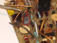
NSD128 - NTE128 -
As you can see the actual device on the board is not marked NSD128 but otherwise. Perhaps it can be better identified by the close-up image?
Thanks All!
Shawn.
krmaudio said:re: nsd128 as far as im aware its a d44, i will get some pics on here of various transistors on the main boards, i currently have 11 dc300a's (dont laugh) 90% are original and all have various transistors fitted, basically no 2 are the same, because lets face it they made several thousand over a period of years i would have thought ........
d40 also crops up (these are available stateside surely?) no special devices, i would have thought much easier to source us than uk!
keep plugging away!
As you can see the actual device on the board is not marked NSD128 but otherwise. Perhaps it can be better identified by the close-up image?
Thanks All!
Shawn.
Attachments

Oh those burn marks sooooo bring back D75 memories
What about those D60 memories?
Shawn,
Do I need to dig up my DC300 service manuals for info?
Nice clear picture by the way. Did you take it?😀
Do I need to dig up my DC300 service manuals for info?
Nice clear picture by the way. Did you take it?😀
burnedfingers said:
What about those D60 memories?
Was it the 35 and 60? Fortunately those are dim memories, the scorch marks recalled only due to sheer repetition. 😉
- Home
- Amplifiers
- Solid State
- Resurrecting a Crown DC300A