Does M2Tech Evo need this ?
As far as i could see it...

An externally hosted image should be here but it was not working when we last tested it.
...it has a buffer behind the I2S connector.
Could someone please advise me as to what value resistor to place across the output of the +5 volt regulator to simulate the Optivol load so that I can set the voltage before connecting up the LDR's. TIA.
Marra
Marra
Could someone please advise me as to what value resistor to place across the output of the +5 volt regulator to simulate the Optivol load so that I can set the voltage before connecting up the LDR's. TIA.
Marra
See reply in OVC thread!
So what's the science behind that? What do R28 and R31 do?
No science, no 'scope, just a bit of luck. DD's module didn't work with Oliver's board so I looked at the input circuitry as that's where Oliver's design differs from others. Somewhere on the threads there's a discussion on this but I can't find it right now.
By-passing R3 in the FS line and R5 in the data line was easy to do but made no difference so I put them back. However, removing the pull up R28 and the pull-down R31 in the BCK line got the circuit working so (this is the clever bit) I left them out. There are probably better solutions but for now it's working.
I'm still wondering what a high-speed buffer is for. Folk who've ordered one presumably know what they want it for: if it's a better solution to this problem than the one I've come up with (i.e. I'm missing the point), I'd like to know . . .
HTH
As far as i could see it...
...it has a buffer behind the I2S connector.
That IC9 chip I guess
I'm still wondering what a high-speed buffer is for. Folk who've ordered one presumably know what they want it for: if it's a better solution to this problem than the one I've come up with (i.e. I'm missing the point), I'd like to know . . .
HTH
Propagation delay, I guess, all things equal almost 3 times lower of 74HC family
I'm still wondering what a high-speed buffer is for.
Steve Nugent of Empirical Audio wrote a large article in the POSITIVE FEEDBACK ONLINE - ISSUE 43
about "Jitter in Digital Audio Data Streams".
I hope this answer your question.
Logic buffering
The digital audio data must make its way through the system over wires/traces and sometimes through buffers,
such as the buffer to drive the S/PDIF cable.
Each of these buffers has finite reaction times and imprecise detection of changing signal levels.
What this means is that even though the signal may not have much jitter coming into the buffer,
it may exit with additional jitter.
This jitter is a result of the speed of the device, thermal effects on the silicon die,
power delivery on the die and even transmission-line effects.
The WM8804 and other I2S converter typical supply voltage equals 3.3V.
The I2S attenuators from ecdesigns i am using on my DAC module, are designed for 5V TTL levels only.
So we need the buffer between the output of these 3.3V devices and the input of my DAC module
for a proper work, without canceling the advantages of the I2S attenuators.
Hi Oliver
Malka07 - 1x
studiostevus - 1x
Crusty - 1x
kamaths - 1x
av-trouvaille - 1x
ernesternest - 1x
noizas - 2x
Malka07 - 1x
studiostevus - 1x
Crusty - 1x
kamaths - 1x
av-trouvaille - 1x
ernesternest - 1x
noizas - 2x
buffer boards
Oliver
From you description an some reading of the article above, where should we put the buffer module actually??? Is it to every digital output such as I2S or spdf from signal source or digital input of a dac ?
Steve Nugent of Empirical Audio wrote a large article in the POSITIVE FEEDBACK ONLINE - ISSUE 43
about "Jitter in Digital Audio Data Streams".
I hope this answer your question.
The WM8804 and other I2S converter typical supply voltage equals 3.3V.
The I2S attenuators from ecdesigns i am using on my DAC module, are designed for 5V TTL levels only.
So we need the buffer between the output of these 3.3V devices and the input of my DAC module
for a proper work, without canceling the advantages of the I2S attenuators.
Oliver
From you description an some reading of the article above, where should we put the buffer module actually??? Is it to every digital output such as I2S or spdf from signal source or digital input of a dac ?
Oliver
From you description an some reading of the article above, where should we put the buffer module actually??? Is it to every digital output such as I2S or spdf from signal source or digital input of a dac ?
The buffer is only needed at the I2S line converter output, if it has no buffer onboard.
I2S Converter --> Buffer --> DAC Module
Data --> Buffer input - Buffer output --> Data DAC module
LRCLK --> Buffer input - Buffer output --> FS DAC module
BCK --> Buffer input - Buffer output --> BCK DAC module
The buffer is only needed at the I2S line converter output, if it has no buffer onboard.
I2S Converter --> Buffer --> DAC Module
Data --> Buffer input - Buffer output --> Data DAC module
LRCLK --> Buffer input - Buffer output --> FS DAC module
BCK --> Buffer input - Buffer output --> BCK DAC module
Thanks for the explanation
So in a nutshell it is an improvement to have a external buffer with a dedicated psu for i2s data and before to a dac since we using a long wires...right?
is this justify why DD i2s to spdf doesn't sound 'well' since it's using on board buffer?
will this practice works well to other dac with i2s source in one board together?
As posted before, the used I2S attenuator on my DAC module is designed for 5V TTL levels.
If you use my DAC module with 3.3V I2S converter IC´s that have no onboard buffer, it won´t work.
Doede has only a SPDIF to I2S converter pcb not vice versa without an onboard buffer, or i missed something. 🙂
BTW, the used I2S connection should be as short as possible, independend from the buffer IC.

Salas Regulator -V Input Connector
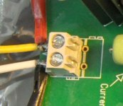
Sorry if this post is not in the correct thread!
There is a small issue using non-Wago terminal board connectors on the Salas shunt regulator that should be known.
If you are using this type of connector (2 solder pin, see picture) instead of 4 (pcb solder) pin (Wago) on the shunt regulator PCB, you must do one of 2 things:
1 - You can solder the terminal block to the REAR set of PCB pins to insure the ground plane is connected.
2 - You can solder the connector to the FRONT set of pins, but be sure to jumper the GROUND pin to the READ GROUND pin connector
For example, if it is connected as the picture shows without performing step 1, there will be no negative voltage on the -15V or -5V outputs
Regards,
Gary
Attachments
As posted before, the used I2S attenuator on my DAC module is designed for 5V TTL levels.
If you use my DAC module with 3.3V I2S converter IC´s that have no onboard buffer, it won´t work.
Doede has only a SPDIF to I2S converter pcb not vice versa without an onboard buffer, or i missed something. 🙂
BTW, the used I2S connection should be as short as possible, independend from the buffer IC.
well said Oliver....sorry for the confusion 😉
Sorry if this post is not in the correct thread!
There is a small issue using non-Wago terminal board connectors on the Salas shunt regulator that should be known.
If you are using this type of connector (2 solder pin, see picture) instead of 4 (pcb solder) pin (Wago) on the shunt regulator PCB, you must do one of 2 things:
1 - You can solder the terminal block to the REAR set of PCB pins to insure the ground plane is connected.
2 - You can solder the connector to the FRONT set of pins, but be sure to jumper the GROUND pin to the READ GROUND pin connector
For example, if it is connected as the picture shows without performing step 1, there will be no negative voltage on the -15V or -5V outputs
Regards,
Gary
Thanks for highlighting. I had not noticed this.
Doede has only a SPDIF to I2S converter pcb not vice versa without an onboard buffer . . .
First, thanks for clarifying the role of the new buffer.
Second, for the record and with apologies for the repetition, the DDDAC “range” includes a USB-to-I2S module that doesn’t have an on-board buffer for the I2S bus and/or an S/PDIF-to-I2S module that does. For obvious reasons (fan-out to between 12 and 60 DAC chips), there is a 74HC125 buffer on each 12-way DAC board. According to the datasheets, its delay is about eight nSecs compared to just under three nSecs for the rather newer NC7SZ125 that Oliver selected.
DD’s USB-to-I2S module cannot drive the TDA1541A on Oliver’s board unless R28 and R31 are removed from the BCK line. If they are, it works fine. However, a better solution might be to reinstate the resistors and use Oliver’s buffer instead even if DD's board does use 5-volt levels. I’m more than happy to try that.
In short, can you put me down for a couple?
Now that Oliver has successfully tested the Tent clock in the Teralink box, the latter's ability to handle 24/96 must mean that it's the device of choice unless constructors already have one of DD’s boards going spare (as I did).
BTW, I see that the Teralink also uses the 74HC125 buffer. It might be interesting to see if replacing it with the NC7SZ125 makes for any improvement . . . 😱
HTH
Dave
In the meantime i have canceled the onboard LC-filter in the +5V line of the standard TCXOBTW, I see that the Teralink also uses the 74HC125 buffer. It might be interesting to see if replacing it with the NC7SZ125 makes for any improvement . . . 😱
HTH
Dave
and changed the 74HC125 to the faster 74VHC125 (3.8ns) HERE.
Not as fast as the NC7SZ125 (2.6ns) and all lines in one chip, but with an interesting result.
The lower end get´s more punch and the stage open up a bit.
The lower end gets more punch and the stage open up a bit.
You got there before me! Interestingly, I've seen both of these effects reported elsewhere as characteristic of reduced jitter. Well done.
I wonder if, for the sake of elderly, ham-handed types like me, it would be possible to cut the old buffer out and run links direct to the new buffer board or even just leave it in place and do the same.
If you have the right equipment (smd solder iron) and experiences with it, trust me it is not easy....
I wonder if, for the sake of elderly, ham-handed types like me, it would be possible to cut the old buffer out and run links direct to the new buffer board or even just leave it in place and do the same.
Cut the legs of the chip. When I replaced my 74CH125 with the 74VHC125 even thought I had a Weller desolder machine just couldn't get the solder out of the holes (double sided pcb, the horror of the diyer 😡)
BTW same results here too, phenomenal soundstage and much clearer sound (DDDAC via DD's USB)
Now, I finally had the time to order the parts for this DAC, building my Mouser list but I wanted to ask if there is any reason why I get into trouble ordering from Partsconnexion the resistors i.e. are PRP resistors better than Dale's RN60/55s ?
Last edited:
- Status
- Not open for further replies.
- Home
- Group Buys
- "Reference" TDA1541A DAC with I2S-BUS architecture