jens:
nice job!
to answer an earlier question, i'd be interested in a couple of boards if you made them available
mlloyd1
nice job!
to answer an earlier question, i'd be interested in a couple of boards if you made them available
mlloyd1
thanks,
Previews with groundplane
Top:
Bottom:
\Jens
Previews with groundplane
Top:
An externally hosted image should be here but it was not working when we last tested it.
Bottom:
An externally hosted image should be here but it was not working when we last tested it.
\Jens
A more standard version.
Please comment
\Jens
Please comment
An externally hosted image should be here but it was not working when we last tested it.
\Jens
JensRasmussen said:A more standard version.
Please comment
An externally hosted image should be here but it was not working when we last tested it.
\Jens
Looks good. I have a few comments:
- for the VBE multiplier diode pcbs, I would add an extra hole on the other side, so you can firmly mount them to the heatsink. A single screw hole might not ensure a good thermal connection.
- As for the driver transistors, I would still go back to using a seperate heatsink for them, or at least make more space to allow using both options, as Dr. Leach said that it was best to isolate them thermally from the output transistors
- As for the grounding scheme, I don't see why you have 3 grounds attached to the ground plane, one from the central ground going into the output trace, and then 1 from each supply rail going from the power supply. I would worry about ground loops if 3 wires are run to the central ground from the pcb. Leach's scheme only had a single central ground wire attached to each ground, where the signal ground and output ground were not tied directly together. I see that you seperated the input grounds and added the R51 resistor, which looks good to me.
- As far as the overall board layout, I would rather see the large capacitors go offboard, and a power supply board created. When the production boards are made, you could have the two boards attached together with scoring. If you move the caps off board (and you could use some local 100uF caps like Leach does), then the board could be smaller. It would be nice to be able to vertically mount the thing in a reasonably sized chassis.
- My opinion is that if you move the large caps off board, along with the fuses, and also decreasing the size of the C24/C25/C29/C30, there would be a way to make a more narrow board. I would consider changing the output resistors to 2 - 3w metal film (panasonics are cheap) in parallel to get the 0.33 ohm value. This would also allow for easier matching of the output resistors if desired (not really need, from what I have heard)
- Also, if the 10000uF (or whatever the big caps are) are moved off board, you could always use some 1500uF 63v caps to put on the board if you wanted something larger than Leach's 100uF recommendation.
- I would think that it would be better to have 3 pairs of output devices. If only 2 pairs were desired, then the middle pair could be omitted, allowing for better spacing of the output devices.
http://www.briangt.com/gallery/leachamppcb
I would someday like to see these things created and put out there. I really like how you have evolved the design.
EDIT:
One more idea would be to change the resistors in the design over to the newer mini 0.5w metal film resistors. I have used these in my gainclone kits, and they are quite small. I have read that the smaller resistors are better, and would allow the design to shrink quite a bit. The highest wattage resistor needed on the leach amp besides the 0.33R output resistors is 0.5w for these 8 resistors:
-resistors tied to voltage rails in the diffamp (13,14)
-resistors in the protection circuit (30,31)
-resistors series with the base of the output transistors (41-44) [are you using 1/4w here?]
The rest are specified as 0.25w
I am referring to the SFR16S resistors by Phoenix on this page:
http://dkc3.digikey.com/PDF/T043/0955.pdf
They measure 0.126" (3.2mm) and easily work with 200 mil spacing. A couple other companies make the same resistor also, digikey also carries the panasonic version of this resistor.
I guess that the layout would have to be reworked though, as with the with 400mil spaced resistors, you have more room to run traces through them.
YET ANOTHER EDIT:
I forgot to mention one more thing, as for including the R50/C25 (leach's designation) for the output filter on the pcb, he says this on his webpage:
"On the first amplifier I built, I had these on the circuit board where they caused violent oscillations because the current through R50 and C25 generated positive feedback when it flowed through the circuit board signal ground lead. When the oscillations occurred, the heat sinks would get very hot. Moving R50 and C25 to the loudspeaker output binding posts solved this problem."
[your C21, R47]
--
Brian
originally posted by BrianGT
As far as the overall board layout, I would rather see the large capacitors go offboard, and a power supply board created.
I agree with Brian on this one.
IMO the benefits of a seperate power supply board would be manifold:
- Mounting multiple amps (active speaker system) on one heatsink would be difficult as the board is now - it "wastes" to much heatsink area (but also for mounting only one PCB the dimensions are a little "unfortunate" regarding choice of mounting/ heatsink/enclosure options) .
- Simplified (better?) routing of power and signal ground.
- As the input stage would be closer to the output transistors, signal traces would be shorter.
- Electrolytic Power Supply caps are a little further away from the heatsink (possibly increased cap lifetime due to lower temperature).
- The power supply board could have the same size as the amp board and it could be easily stacked directly on top of it. Fat metal srew standoffs could connect the power-supply board to the amp-board providing electrical and mechanical connection of the two boards. This way the distance from power supply caps to output transistors wouldn`t be any larger as it is now. For that reason additional (electrolytic) power supply bypass caps on the amp board near the output transistors maybe even omitted at all.
Hello,
Thanks for all the construktive comments.
Brian:
· for the VBE multiplier diode pcbs, I would add an extra hole on the other side, so you can firmly mount them to the heatsink. A single screw hole might not ensure a good thermal connection.
You are right. I will change it so the small PCB has a 3.2 mm hole in each end to accomodate the need for good thermal contact.
· As for the driver transistors, I would still go back to using a seperate heatsink for them, or at least make more space to allow using both options, as Dr. Leach said that it was best to isolate them thermally from the output transistors
I will make space for this option.
· As for the grounding scheme, I don't see why you have 3 grounds attached to the ground plane, one from the central ground going into the output trace, and then 1 from each supply rail going from the power supply. I would worry about ground loops if 3 wires are run to the central ground from the pcb. Leach's scheme only had a single central ground wire attached to each ground, where the signal ground and output ground were not tied directly together. I see that you seperated the input grounds and added the R51 resistor, which looks good to me.
Well, I wanted to make a central gnd connection close to the big caps on the board. Depending on the way you route the wires in the cabinet you could have the central gnd connection on one side or the other. The gnd connection by the output was intendeed for output only. It’s ment as an option, nothingmore.
· As far as the overall board layout, I would rather see the large capacitors go offboard, and a power supply board created. When the production boards are made, you could have the two boards attached together with scoring. If you move the caps off board (and you could use some local 100uF caps like Leach does), then the board could be smaller. It would be nice to be able to vertically mount the thing in a reasonably sized chassis.
I like a compact unit and short traces for the rails.
I’ll have to make a drawing to show what my intentions are for the mechanical layout of the box.
· My opinion is that if you move the large caps off board, along with the fuses, and also decreasing the size of the C24/C25/C29/C30, there would be a way to make a more narrow board. I would consider changing the output resistors to 2 - 3w metal film (panasonics are cheap) in parallel to get the 0.33 ohm value. This would also allow for easier matching of the output resistors if desired (not really need, from what I have heard)
You are right, regarding the emitter resistors, but I’m planning to use non inductive 5W types (don’t remember the brand right now – sorry) I like having fuses on every amp module, just for safety.
· Also, if the 10000uF (or whatever the big caps are) are moved off board, you could always use some 1500uF 63v caps to put on the board if you wanted something larger than Leach's 100uF recommendation.
I want to use at least 80V types for the caps, the ones on the board now are 10000uF 100V
· I would think that it would be better to have 3 pairs of output devices. If only 2 pairs were desired, then the middle pair could be omitted, allowing for better spacing of the output devices.
Nice idear, I will change it.
As for resistors i will look into the smaller models, bu I like using standard components that are easy to get i most places. Thus the choises made so far. The base resistors ¼ watt types but need to be changed (the are ¼ in my running prototype with 5 output transistors)
· I forgot to mention one more thing, as for including the R50/C25 (leach's designation) for the output filter on the pcb, he says this on his webpage:
I have the zobel network on my prototype board, and have had no problems with oscillations. Maybe the gnd plane makes a difference here?
Christoph
· Mounting multiple amps (active speaker system) on one heatsink would be difficult as the board is now - it "wastes" to much heatsink area (but also for mounting only one PCB the dimensions are a little "unfortunate" regarding choice of mounting/ heatsink/enclosure options) .
The board is designed to fit i a 3u 19 inch box.
I will work out a new layout and post it here ASAP (I'm wisiting family at the moment and starting a new job on monday so I’m a littel busy)
Thanks for the idears - keep them comming! 🙂
\Jens
JensRasmussen
Your PCB looks even better than some of the best , conguratulations !!!
Please let me have the value of resistors in the protection ckt you have used for five pairs of output transistors .
Thanks
Rajeev
Your PCB looks even better than some of the best , conguratulations !!!
Please let me have the value of resistors in the protection ckt you have used for five pairs of output transistors .
Thanks
Rajeev
Hello,
The values will depend on what rail voltages you use.
Also the protection is slightly modded, as I ues a measurement on each emitte resistor to feed the protectection transistor.
What are your rails?
\Jens
The values will depend on what rail voltages you use.
Also the protection is slightly modded, as I ues a measurement on each emitte resistor to feed the protectection transistor.
What are your rails?
\Jens
Jens ,
Thanks for the reply
If you let me know your supply voltage and resistor values and speaker impedance , I will calculate mine on basis of yours ,
However if you will do it for me , the supply voltage is +/- 90v and 8 pairs of 2SA 1943 /2SC 5200 , and min speaker impedance 2 ohms , normally I will use it at 4 ohms .
It is the Leach Amp design .
Rajeev
New pics
Board is 110 x 206 [mm]
\Jens
JensRasmussen said:
Previews with groundplane
Top:
An externally hosted image should be here but it was not working when we last tested it.
Bottom:
An externally hosted image should be here but it was not working when we last tested it.
\Jens
Board is 110 x 206 [mm]
\Jens
Hi Jens, great board! I would also be interested in a group buy if you plan on it.
Just a couple of suggestions, sorry if this has been mentioned earlier in the thread:
1. Move the output coil and output connector to between R48 and C22. This way you get a clean pick-up point for the feedback signal. This is in D. Self's distortion articles (number 7?). Now it should be easier to make a star ground with the output connector and the big caps.
2. Be very careful about placement of the feedback resistors. Their ground-connection should be very close to input ground. the input-connector doesn't necessarily need to be on the edge of the board!
Hello,
Sorry for the delay, I have been busy at work.
I’m not changing the overall layout of the board anymore than maybe a few minor details.
The feedback signal refers to signal ground, witch refers to power ground through a 10 ohm resistor. This should be ok with respect to noise.
I hope to order prototype boards soon.
\Jens
Jens Rasmussen,
I was just wondering if you had a chance to compare your modified leach amp and the original, and if you noticed any differences? With that many changes it should have some type of effect.
I was just wondering if you had a chance to compare your modified leach amp and the original, and if you noticed any differences? With that many changes it should have some type of effect.
Hello,
I have only listened to my own version of the amp, but have simulated a better bass response and lower open loop gain in my version.
Boards not ordered yet, as I have some layout ideas I want to try out before I order.
\Jens
I have only listened to my own version of the amp, but have simulated a better bass response and lower open loop gain in my version.
Boards not ordered yet, as I have some layout ideas I want to try out before I order.
\Jens
I have a few suggestions you may want to try out.
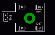
For the temp sensing board, In order to get the board to lay down better on the device, I would try making it out of brick shaped (flat) surface mount diodes, placed symmetrically around the mounting hole. You may also want to include too of these boards connecting two diodes, and two diodes, just in case some one wants to use a different heat sinks for the n and p types.
So that the, main board can assert even pressure on the output transistors you may want to move any through hole devices off of the top of the output devices.
Leve
Attachments
Some of us can and do. Even the old fogeys. Magnifying lighted lens helps. Not too much coffee.
Prosit Not too much of this either.
Prosit
Not too much of this either.- Status
- Not open for further replies.
- Home
- Amplifiers
- Solid State
- redesign of leach amp pcb for integrated TO-247 output devices