As far as I know you can alwas go higher. The only difference is the max reverse voltage required to blow them up. 1N4004 can withstand 400V, I think. 1N4007 up to 1kV. Either of these look like an adequate margin of safety for anything I deal with. (If I thought they might not be, I might reconsider my invovlment!)
4007 replaces 4001...4006
Hello ,
of course you can replace 4005 diode by 4007 , the 4007 is the same but for higher voltage (i think until 1000V by 1A)
Hello ,
of course you can replace 4005 diode by 4007 , the 4007 is the same but for higher voltage (i think until 1000V by 1A)
Thanks, that's a big help.
I wasn't sure if the greater voltage made any difference. I wonder why companies don't just use the 4007 for everything. It didn't seem as thought the cost was much greater at all.
Blessings, Terry
I wasn't sure if the greater voltage made any difference. I wonder why companies don't just use the 4007 for everything. It didn't seem as thought the cost was much greater at all.
Blessings, Terry
...depends...
...If the diode is forward biased the differences are minimal, reverse biased, the capacitance of the higher voltage part is necessarily different...
I wouldn't worry for any normal use, but conceivably it could matter for some things...
Stuart
...If the diode is forward biased the differences are minimal, reverse biased, the capacitance of the higher voltage part is necessarily different...
I wouldn't worry for any normal use, but conceivably it could matter for some things...
Stuart
Can anyone explain to me why the value of R13 and R14 (in the original document of Dr. Leach) is (v-40)/8.2?
Why not use the to220 package diodes instead of the original thermal compensation diodes? They are more costy, but not much. They can be easily bolted to the main heatsink, reacts better to thermal variation, and no need for the small board.
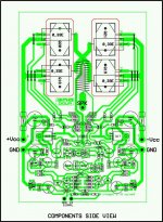
I have made some modifications to the pcb layout of Jens with Orcad but don't know how to export the layout to clear image files so that I can show them in the forum like Jens did.
I have made some modifications to the pcb layout of Jens with Orcad but don't know how to export the layout to clear image files so that I can show them in the forum like Jens did.
I decided against the TO-220 diodes, because I found that the layout could be made tighter with the small PCB on the Heatsink.
Also I'm not sure about the capacity from the diode to the heatsink in the bigger TO-220 box.
Keep us updated on your progress please 🙂
\Jens
Also I'm not sure about the capacity from the diode to the heatsink in the bigger TO-220 box.
Keep us updated on your progress please 🙂
\Jens
EJ said:Can anyone explain to me why the value of R13 and R14 (in the original document of Dr. Leach) is (v-40)/8.2?
40 volts is the input voltage for the current source, this is set by two 20 volt zener diodes.
This means the voltage drop over R13 and R14 in the original Leach doc. is: V-40
The 8.2 reads as 8.2 mA, this is the total current going through Q2,Q3 and Q4 of the two entrance current mirrors.
These currents are determined for the optimum of bandwidth(linearity), and signal to noise.
The higher the current through a transistor the more linear a device becomes.
Downside: higher dissipation, higher current creates higher noise level.
Those figures can be read from a datasheet.
As R= V/ i>> R13= voltagedrop divided current through R13.
If another PS voltage is desired the current through the entrance transistors should remain the same for optimum performance, thus R13 and R14 need to be changed.
jacco vermeulen said:
40 volts is the input voltage for the current source, this is set by two 20 volt zener diodes.
This means the voltage drop over R13 and R14 in the original Leach doc. is: V-40
The 8.2 reads as 8.2 mA, this is the total current going through Q2,Q3 and Q4 of the two entrance current mirrors.
These currents are determined for the optimum of bandwidth(linearity), and signal to noise.
The higher the current through a transistor the more linear a device becomes.
Downside: higher dissipation, higher current creates higher noise level.
Those figures can be read from a datasheet.
As R= V/ i>> R13= voltagedrop divided current through R13.
If another PS voltage is desired the current through the entrance transistors should remain the same for optimum performance, thus R13 and R14 need to be changed.
Thanks, Jacco. I think I understand now. So....
We are having 40V/12kohm=3.33mA through R15, and 3.33mA/2=1.67mA through Q2, which makes the current througn D13 and D14 = 8.2mA-3.33mA-1.67mA = 3.2mA, right?
JensRasmussen said:I decided against the TO-220 diodes, because I found that the layout could be made tighter with the small PCB on the Heatsink.
Also I'm not sure about the capacity from the diode to the heatsink in the bigger TO-220 box.
Keep us updated on your progress please 🙂
\Jens
Hi Jens,
How did you generate those images with such fine quality? I'm still struggling to generate the image files from my layout.

The to220 diodes will not increase the board size very much because they are beneath the board and other parts can be placed over the diodes, just like the way you place the base resistors over the output transistors. I measured the dimension of my layout. It's 4.4 inches by 9.55 inches, which is equal to 11.76cm*24.26cm, very close to yours.
here is the placement
EJ said:We are having 40V/12kohm=3.33mA through R15, and 3.33mA/2=1.67mA through Q2, which makes the current througn D13 and D14 = 8.2mA-3.33mA-1.67mA = 3.2mA, right?
Not quite.
You have +40v on the base of Q5, -40v on the base of Q6.
Thats 80 volts.
R15+R9+R10, and R7+R8+R16 have 80volts minus the voltage drop from collector to emitter of Q1+Q2,Q3+Q4 over them.
I forgot to mention that the part designation are exactly the same as Jans', except that the transistors are designated as "Q?" instead of "T?".EJ said:
Hello,
Would these devices work in the "leach" amp: MJL21196/MJL21195?
If they work should I do any corrections to other parts?
I didn't read the whole story so don't judge me
Would these devices work in the "leach" amp: MJL21196/MJL21195?
If they work should I do any corrections to other parts?
I didn't read the whole story so don't judge me
Hello people!
Here is my version of Leach amplifier PCB with two pairs of Sanken's 2SC3858 / 2SA1494. If anyone is interested, I can post components layout too. My version is working on +/-58V and with unconditional stability.
Bora www.bas.abshost.net
Here is my version of Leach amplifier PCB with two pairs of Sanken's 2SC3858 / 2SA1494. If anyone is interested, I can post components layout too. My version is working on +/-58V and with unconditional stability.
Bora www.bas.abshost.net
Attachments
boraomega said:Here is my version of Leach amplifier PCB with two pairs of Sanken's 2SC3858 / 2SA1494. www.bas.abshost.net
Dr Boraomega,
did you make any other changes other than the MT200's ?
TV Hero, if you've seen the datasheet of the MJL21196/MJL21195, you'd know they are good replacements, i believe soa of these is 4 amps at 100vce.
Here is the layout. Sorry, no photos for now. I've done it for another man and I 'll try to ask him to make some pics if he is willing.
Sorry for less than perfect JPG, but forum limit is 100KB and 1000x1000pixels. Higher resolution GIF I can send as an attachment to E-mail if neccessary.
Sorry for less than perfect JPG, but forum limit is 100KB and 1000x1000pixels. Higher resolution GIF I can send as an attachment to E-mail if neccessary.
Attachments
I've done some changes:
*All "small" transistors, (Q1...Q11) are 2N5401/2N5551 and PCB is designed for that pinout (swapped C & E compared to standard BC series transistors).
*Q12.... Q17 are as in original specification.
*Output's are 2SC3858 / 2SA1494. To me, probably best overall choice regarding ruggedness, reliability, power and heat transfer surface.
I've done two Leach amps, both for other people that requested specifically that amp, and in a first one output devices were MJL3281/MJL1302, that also worked marvelously. I developed PCB for stereo version using that case (TO247), and I can post it too if there is any interest.
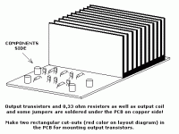
PCB-Heatsink-output transistors assembly might not be entirely clear and obvious for some people, therefore I've done some coarse drawing in attempt to clarify that.
*All "small" transistors, (Q1...Q11) are 2N5401/2N5551 and PCB is designed for that pinout (swapped C & E compared to standard BC series transistors).
*Q12.... Q17 are as in original specification.
*Output's are 2SC3858 / 2SA1494. To me, probably best overall choice regarding ruggedness, reliability, power and heat transfer surface.
I've done two Leach amps, both for other people that requested specifically that amp, and in a first one output devices were MJL3281/MJL1302, that also worked marvelously. I developed PCB for stereo version using that case (TO247), and I can post it too if there is any interest.
PCB-Heatsink-output transistors assembly might not be entirely clear and obvious for some people, therefore I've done some coarse drawing in attempt to clarify that.
Attachments
- Status
- Not open for further replies.
- Home
- Amplifiers
- Solid State
- redesign of leach amp pcb for integrated TO-247 output devices