Hello
The is a thread about a high performance amplifier called the Phoenix .
>The values of the freq. comp. components are cc9 = 1nF & rc9 = 56R.
BTW, they don't compensate Q16/16, rather Q22/23.
Are these values for the output stage stability of Q22/Q23.
>Regarding the temp. compensation, it's a bit tricky with this design. The point is that the loading on the VAS output should be kept as low as possible. Even a small capacitance of 10pF has already an effect on the performance. Now imagine what a classical Vbe multiplier will do, a TO126 tranny that is mounted on the heat sink...... Right!
Also, we have issues with the thermal delay.
When you are talking about the output loading of the VAS are you talking about the capacitance of the TO126 tranny would introduce when it is connected to the heatsink (GND). So it forms a capacitor from the VAS stage to ground - is this what you mean ?.
The thermal track diodes of the NJL4281/4302 wouldnt they introduce a similar capacitive loading also.
Regards
Arthur
Attachments
Hello
The is a thread about a high performance amplifier called the Phoenix .
>The values of the freq. comp. components are cc9 = 1nF & rc9 = 56R.
BTW, they don't compensate Q16/16, rather Q22/23.
Are these values for the output stage stability of Q22/Q23.
Hi Arthur,
Something went wrong, as the component names have changed in the meantime.
Looking at the latest schematic I mean Q15/16 (again). But actually, it compensates the whole OPS (only when clipping, of course).
>Regarding the temp. compensation, it's a bit tricky with this design. The point is that the loading on the VAS output should be kept as low as possible. Even a small capacitance of 10pF has already an effect on the performance. Now imagine what a classical Vbe multiplier will do, a TO126 tranny that is mounted on the heat sink...... Right!
Also, we have issues with the thermal delay.
When you are talking about the output loading of the VAS are you talking about the capacitance of the TO126 tranny would introduce when it is connected to the heat sink (GND). So it forms a capacitor from the VAS stage to ground - is this what you mean ?.
Yes.
The thermal track diodes of the NJL4281/4302 wouldn't they introduce a similar capacitive loading also.
Regards
Arthur
Regrettably, the data sheet don't specify this capacitance, but I assume it's much smaller. However, this isn't an issue any longer, as I have moved these diodes to next stage (pre-driver), where they can do far less harm. I'm still busy with the temp. compensation. The bad news is that it is over compensated. That's really weird, as the TC of the diodes is lower than the Vbe-TC of the O/P trannies, which should result in under compensation. BTW, you also should have a look at this thread: http://www.diyaudio.com/forums/solid-state/71534-semi-thermaltrak.html#post813069
The good news is that it is probably easier to reduce the compensation of an over compensated circuit than vice versa.
I'm away this weekend, so till Monday.
Cheers,
E.
Q1 and Q2
Hello Edmond
Q1 an Q2 supply current , but what problem are you addressing with them.
Regards
Arthur
Hello Edmond
Q1 an Q2 supply current , but what problem are you addressing with them.
Regards
Arthur
Hi Arthur,
Q1 & Q2 are normally off. When the output protection kicks in (which shortens the VAS output), these trannies limits the max. VAS current to about 20mA, otherwise this current will rise to a dangerous 40mA. Also a few other unwanted side effects are suppressed in this way.
In the meantime I discovered an error in the op-amp model. The one we were using so far, is for dual op-amps. Consequently, the supply current is two times as high (10mA instead of 5mA). See also: http://www.diyaudio.com/forums/software-tools/101810-spice-simulation-98.html#post2316573
So I had to modify not only the model but also the schematic. I also played with the ThermalTrak trannies. Results were very encouraging and I will soon drop the schematic of the new version (please, have a little patient with me).
Cheers,
E.
edit > otherwise this current will rise to a dangerous 40mA.
should read as: otherwise this current will rise to a dangerous 70mA.
should read as: otherwise this current will rise to a dangerous 70mA.
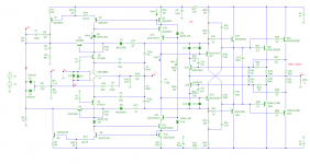
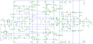
Phoenix7
Hi Arthur,
Here's the new version. Regrettably I don't have correct models of TT-trannies NJL4281/4302 (though I do have models of the TT-diodes). So for the moment, I'm still using the Sanken models.
Please have careful look, in particular at D19 and D20. This clever configuration (courtesy of Bob Cordell) greatly reduces cross-conducting during fast transients.
Don't hesitate to put your questions (probably many 😉 ).
Cheers,
E.
PS: TDH20k is about 1ppm.
Q16 & Q19, respectively Q17 & Q20 are thermally coupled.
Attachments
More on D19 & D20. This is what Bob Cordell said about it:
"The two “extra” ThermalTrak diodes, D3-4, are used between the emitters of the driver transistors to establish the idle current of the drivers while keeping the impedance between the emitters very small, so that the drivers can operate in push-pull to provide turn-on and turn-off current to the output transistors. Keeping the impedance between the driver emitters very low at high frequencies is essentially what is often done with the speedup capacitor. The ThermalTrak diodes make it possible to do this in a d.c. fashion with the necessary precision because they track the output transistor Vbe’s. "
See also: http://www.diyaudio.com/forums/soli...ion-thermal-trak-transistors.html#post1264875
I would highly recommend this scheme.
And below a compilation of some comments, graphs and schematics about the ThermalTrak trannies and diodes.
Cheers,
E.
Attachments
Hello Edmond
Sorry I have not posted any questions yet, but I am just playing around with the most recent circuit (Pheonix7) to get some idea of all the things that you have done , it has lots of nice tricks. The output stage protection is is really nice the way it pulls the current away from the predrivers q16 and q17 in protection mode . Also the main clamp transistors q13 and q14 are also connected differently than in Pheonix6.
Here is a question though why have you connected the collector of Q1 with the collector of Q13.
More questions will follow.
Regards
Arthur
Hello Edmond
Sorry I have not posted any questions yet, but I am just playing around with the most recent circuit (Pheonix7) to get some idea of all the things that you have done , it has lots of nice tricks.
Hi Arthur,
Indeed, many trick and many changes. Please take your time to digest them.
The output stage protection is is really nice the way it pulls the current away from the predrivers q16 and q17 in protection mode . Also the main clamp transistors q13 and q14 are also connected differently than in Pheonix6.
That's right. Q13 & Q14 are biased form other sources, i.e. from outside the signal path. As a result, slightly less distortion.
Here is a question though why have you connected the collector of Q1 with the collector of Q13.
More questions will follow.
Regards
Arthur
Similar to Q13 & Q14, Q1 & Q2 also function as an active feedback clamp, this time to limit the VAS peak current. Hence the collectors are tied to the same node (U) in order to provide feedback. Without this FB, currents through the op-amp and Q3...Q12 would rise to unacceptably high levels when the OP protection kicks in.
In the coming days, I will describe step by step the various function and (protective) FB loops, together with graphs of the phase and gain margin.
Cheers,
E.
Version 8
Hi Arthur,
the project experiences some delay as I'm busy with a new version. This one has improved current mirrors: lower distortion and (slightly) more output swing, only 2V below the supply rails. It's also based on a Wilson current mirror, tough combined with another trick of Hawksford instead of his cascode. See his AES paper: "Reduction of Transistor Slope Impedance Dependent Distortion in Large-Signal Amplifiers", p.217, Fig. 5b.
Furthermore, the circuit is slightly less complex: the green LEDs are gone.
Cheers,
E.
Hi Arthur,
Here's version 8, together with a MC9 file.
The following changes are:
1. Better and simpler current mirrors (Q7 & Q8).
2. Miller compensation of the 'Wilson loop' (C5 & R20, C7 & R21)
3. Different protection of the current mirrors (Q1 & Q2)
4. Constant current sources for the diamond driver (Q15 & Q18)
5. D11 & D12 crosswise connected to Q16 & Q17.
6. Added input filter and supply rails filters.
7. Added Zobel network
THD = 1.4ppm @ 20kHz, 200W into 4 Ohms, BW = 100kHz.
If OPS protection disabled: THD20 = 1.1ppm
If OPS protection disabled and ideal op-amp: THD20 = 0.4ppm
To do : plus & minus 15V PSU
Cheers,
E.
Attachments
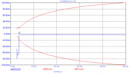
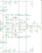
biasing the output stage
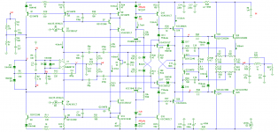
Hi Arthur,
At first glance, biasing the output stage with ThermalTrack trannies and diodes (1st pic below, D7 & D8) looks very promising. However, I encountered a few problems:
If the diamond driver gets its supply current as shown here (by means of R23...R26, C8 & C9), the bias current depends on the supply voltage, see 2nd pic below. I assume you don't like this (unless you are using a regulated PSU, of course). So I've replaced above passive components by constant current sources (Q13 & Q14) and current mirrors (Q17 & Q19, resp. Q18 & Q22). Now the bias current is far more constant, at least above 19V, see 3rd pic.
So far so good. BUT... these sims are based on models of the Sanken O/P trannies, as I don't have them of the NLJ4281D/4302D pair*. Using similar device models, i.e. of NJL1302D/3281D**, reveals another problem, see next post.
edit: * I don't thrust MODPEX cr@p: VAF=10. Crazy!!!
** These models are also from above idiot, but modified/improved by Andy. Hope they are sufficiently reliable.
Attachments
Last edited:
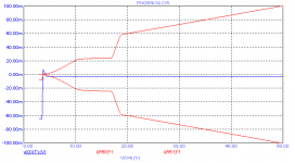
biasing the output stage
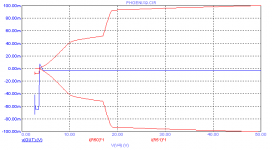
Above problem, i.e. bias dependence on supply voltage, reappears when using NJL1302D/3281D models, see 1st pic. One of the reasons might be that these trannies have a much lower Early voltage, at least according the models: 38 resp. 40V. But how real are these figures? And equally important, where to get reliable models?
Now that it seems impossible to keep the bias setting constant at varying supply voltages, I wonder whether it's worth to spend another 6 trannies for the CCSes and CMs.
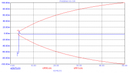
So, let's also have a look at the bias variation of the previous and simpler circuit (based on four Rs and two Cs), see 2nd pic. As we can see, the variation is higher, of course, but not that much: 'only' 50%. So what to do, as none of the circuits is perfect. Should we take this dependence for granted?
Now it's your turn Arthur, please.
One more thing about fine tuning of the bias. Since the TT trannies have a lower Vbe than the Sanken counter parts, I had to connect the bases of the diamond driver crosswise to the trim pot, see jumpers.
Cheers,
E.
Above problem, i.e. bias dependence on supply voltage, reappears when using NJL1302D/3281D models, see 1st pic. One of the reasons might be that these trannies have a much lower Early voltage, at least according the models: 38 resp. 40V. But how real are these figures? And equally important, where to get reliable models?
Now that it seems impossible to keep the bias setting constant at varying supply voltages, I wonder whether it's worth to spend another 6 trannies for the CCSes and CMs.
So, let's also have a look at the bias variation of the previous and simpler circuit (based on four Rs and two Cs), see 2nd pic. As we can see, the variation is higher, of course, but not that much: 'only' 50%. So what to do, as none of the circuits is perfect. Should we take this dependence for granted?
Now it's your turn Arthur, please.
One more thing about fine tuning of the bias. Since the TT trannies have a lower Vbe than the Sanken counter parts, I had to connect the bases of the diamond driver crosswise to the trim pot, see jumpers.
Cheers,
E.
Attachments
DC Servo
Hello Edmond
I think this amp needs a DC servo and do you think it should be placed outside the input wilson CM stage to reduce the power dissipation of Q8 and Q9, or outside with its own crude supply.
On the issue of bias drift with supply rail variation this is your concern , how solid do you think it needs to be or more to the point with Mosfets and associated bias circuitry how much better is it.
I think we are at a stage where I have to build some hardware and get some measured results.
Regards
Arthur
OPS bias
Hi Arthur,
Whether we need a servo depends on the choice of op-amp in the front end. With a LME49710, we don't need a servo at all, as Vos, Ios and Ib are very low. With a AD797 for example, it's different story, as the input bias current (Ib) is much higher.
Biasing MOSFETs is less critical, but then we are talking about a radical different amp. I mean: Optimizing an amp with MOSFETs in the OPS leads to a different design than in case of BJTs in the OPS. As a matter of fact, I don't like BJTs at all, except the NJL4281/4302 pair (NOT NJL1302/3281), as the TT-diodes pave the way to better bias stability (at least in principle).
How solid it needs to be? Partly, this question falls under the same category as 'how much distortion do you accept'. OTOH, in case of a stable and regulated Vcc/Vee it's a non-issue. But in case of a non-regulated PSU, it also depends on the stability of the mains: +10%/-20%? I don't know. As far as I know, you don't have plans for a regulated PSU, do you? So I would say: make it as best as possible, though within reasonable limits in terms of cost and complexity. To give a more clear answer, I think that the Ibias/Vcc dependence as shown in the previous post is not acceptable. So it has to be improved.
That's exactly what I was thinking. At this stage, there are several uncertainties.
As for the op-amp: How large is the spread of the supply current ? That is, lot to lot, and at different temperatures.
As for TT-trannies: How large is VBE of the TT-trannies WRT VFWD of the TT-diodes?
According to measurements by jgedde VBE is around 0.73V at 100mA and 27ºC, but at which Vce? (He didn't mention it, afaik.) Furthermore, the data sheet says 0.6V, again, at which Vce? Rather confusion.
Then there's a lot of discussion on this forum about the misalignment of the diode-TC vs BJT-TC, which in turn also depends on IFWD and Ic. Despite all this, according jgedde (thanks John) it seems that IFWD=7mA should give a perfect tracking. Let's hope this is correct, though my sims predict a lot of overcompensation (probably due to wrong models).
BTW, there's one more error source that has an effect on the Vcc/Ibias dependence: R18 & R19. The higher Vcc and/or Vee, the higher the current through these Rs (of course) and the lower the VAS current. Now comes the crux: if it appears that we need a positive bias voltage between the base of Q20 and Q21 (i.e. NOT crosswise connected to the trim pot, rather 'normally' tied), then we can compensate for the Vcc/Ibias dependence by using the voltage drop across the trim pot to our benefit, at least to a certain extent. Whether this scheme is feasible depends VBE vs VFWD of the TT devices. If VBE > VFWD then it might work. If VBE < VFWD, so we need the 'crosswise connection', this scheme works the wrong way (it worsens the Vcc dependence) and I have to devise something else.
As you see, regarding the final design details, much depends on exact data, i.e. real measurements. Maybe John (alias jgedde) can also shed some more light on this matter, please John!
Cheers,
E.
Hello Edmond
I think this amp needs a DC servo and do you think it should be placed outside the input wilson CM stage to reduce the power dissipation of Q8 and Q9, or outside with its own crude supply.
Hi Arthur,
Whether we need a servo depends on the choice of op-amp in the front end. With a LME49710, we don't need a servo at all, as Vos, Ios and Ib are very low. With a AD797 for example, it's different story, as the input bias current (Ib) is much higher.
On the issue of bias drift with supply rail variation this is your concern, how solid do you think it needs to be or more to the point with Mosfets and associated bias circuitry how much better is it.
Biasing MOSFETs is less critical, but then we are talking about a radical different amp. I mean: Optimizing an amp with MOSFETs in the OPS leads to a different design than in case of BJTs in the OPS. As a matter of fact, I don't like BJTs at all, except the NJL4281/4302 pair (NOT NJL1302/3281), as the TT-diodes pave the way to better bias stability (at least in principle).
How solid it needs to be? Partly, this question falls under the same category as 'how much distortion do you accept'. OTOH, in case of a stable and regulated Vcc/Vee it's a non-issue. But in case of a non-regulated PSU, it also depends on the stability of the mains: +10%/-20%? I don't know. As far as I know, you don't have plans for a regulated PSU, do you? So I would say: make it as best as possible, though within reasonable limits in terms of cost and complexity. To give a more clear answer, I think that the Ibias/Vcc dependence as shown in the previous post is not acceptable. So it has to be improved.
I think we are at a stage where I have to build some hardware and get some measured results.
Regards
Arthur
That's exactly what I was thinking. At this stage, there are several uncertainties.
As for the op-amp: How large is the spread of the supply current ? That is, lot to lot, and at different temperatures.
As for TT-trannies: How large is VBE of the TT-trannies WRT VFWD of the TT-diodes?
According to measurements by jgedde VBE is around 0.73V at 100mA and 27ºC, but at which Vce? (He didn't mention it, afaik.) Furthermore, the data sheet says 0.6V, again, at which Vce? Rather confusion.
Then there's a lot of discussion on this forum about the misalignment of the diode-TC vs BJT-TC, which in turn also depends on IFWD and Ic. Despite all this, according jgedde (thanks John) it seems that IFWD=7mA should give a perfect tracking. Let's hope this is correct, though my sims predict a lot of overcompensation (probably due to wrong models).
BTW, there's one more error source that has an effect on the Vcc/Ibias dependence: R18 & R19. The higher Vcc and/or Vee, the higher the current through these Rs (of course) and the lower the VAS current. Now comes the crux: if it appears that we need a positive bias voltage between the base of Q20 and Q21 (i.e. NOT crosswise connected to the trim pot, rather 'normally' tied), then we can compensate for the Vcc/Ibias dependence by using the voltage drop across the trim pot to our benefit, at least to a certain extent. Whether this scheme is feasible depends VBE vs VFWD of the TT devices. If VBE > VFWD then it might work. If VBE < VFWD, so we need the 'crosswise connection', this scheme works the wrong way (it worsens the Vcc dependence) and I have to devise something else.
As you see, regarding the final design details, much depends on exact data, i.e. real measurements. Maybe John (alias jgedde) can also shed some more light on this matter, please John!
Cheers,
E.
Last edited:
quirk
Hi Arthur,
Now I see what you mean. Indeed, that's a very strange quirk. I never thought that could happen. Anyhow, Q27 & Q29 are NPNs of course and the collectors are connected to +50V.
Cheers,
E.
Hi Arthur,
Now I see what you mean. Indeed, that's a very strange quirk.
I never thought that could happen. Anyhow, Q27 & Q29 are NPNs of course and the collectors are connected to +50V.Cheers,
E.
- Status
- Not open for further replies.
- Home
- Amplifiers
- Solid State
- Rebirth of the Phoenix