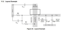
No, no, by spreading the ground, we are just trying to ensure that all the remaining copper is made available for the ground net out of which, the electrically nearest path would be taken by the ground currents that flow. Besides, that is the only thing one could possibly do when working with a single-sided PCB. The more preferred method is to add a plane layer on the component side of the board, as mentioned earlier. However, that becomes a double-sided board.......if the gnd is all around the components " wouldn't that create ground loop ? Which is bad.?.
Another question, are these generic yellow caps good for this design,
The yellow ones are boxed polyester (film) capacitors, often seen on tone control boards. If the wimas are polypropylene, use them.Do you know what type they are - not such thing as a generic cap really, lots of different dielectrics, construction types, etc etc. They look like some sort of plastic film - but what? Mylar? PP?
Last edited:
Double-sided boards can be made at low prices now, so it's a good option.

MKT caps are fine for audio coupling decoupling & i also see some good low value ceramics there with 5% tolarence.
@newvirus2008 I will do the PCB again, thank you !. I don't know about the wima's , took one apart, they are rolled , thin plastic like with alu foil.
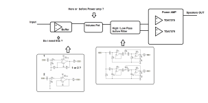
Is this the correct way of implementing Volume control ?. Do i need a buffer before the high low passs filters? .
I might use this https://sound-au.com/project01.htm
I might use this https://sound-au.com/project01.htm
Attachments
Who said that? COG ceramics are excellent for audio & you can use such type in your xover design. The problem is good ceramics are rare & expensive in high values. Similar like polystyrene. Interestingly COG MLCCs are very fragile by construction but not as heat sensitive as polystyrene(if i recall correctly).@NanoFarad Aren't ceramics bad for audio ?.
That's is a wise choice, but don't worry, it shoudn't take a long time to place / route such simple circuits.I will do the PCB again, thank you !.
You can use the yellow box types, I've seen them in countless designs including those from reputed brands. Besides I've also used them to make MFB filters, much similar to what you're doing.I don't know about the wima's , took one apart, they are rolled , thin plastic like with alu foil.
Yes, but that is if you use lousy ceramic type like X7R, X5R, Z5U, Y5V etc. These types are only good for power supply duty & as you know there isn't any better alternative than ceramic for high frequency filtering.@NanoFarad idk, read somewhere ceramics act as " piezo microphones" they have bad liniarity etc.
The point is standard 1oz copper is about 0.5 milliohms per square, so the IR voltages are kept very low compared to standard traces and component leads (although proper star grounding is ideal, a plane can be very good - but don't break it up!).@newvirus2008 " Try to spread the ground around the unused parts, if the gmd is all around the components " wouldn't that create ground loop ? Which is bad.?.


@newvirus2008
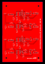
Uploaded also as PDF for better quality if zoomed.
Uploaded also as PDF for better quality if zoomed.
- Should I use separate GND for op amp rails, ( C-1 C+1 , C-2, C+2 ) or
- Just remove them, and use one cap per op amp from pin 4 to 8 ?.
Attachments
Last edited:
I think it would work alright (provided there're no other errors) but you could always rotate C1, C3, C4, C6, R8 etc. and make the board smaller. C2 may also fit above the opamp bringing R3, C3 etc. closer ... well, if you like..
One solid uninterrupted ground fill would suffice for such applications. However, you need to provide decoupling for both supplies with two capacitors. You may add a cap from + to - but that would not make much difference in analogue circuits.
One solid uninterrupted ground fill would suffice for such applications. However, you need to provide decoupling for both supplies with two capacitors. You may add a cap from + to - but that would not make much difference in analogue circuits.
@newvirus2008 Any benefit for being smaller ? ( besides less material wasted ) .
- What about the power supply decoupling caps ? should I let them there or just use one cap per op amp from - to + ( pin 4 - 8 ) ?.
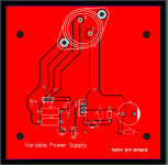
-Since you're here , please also take a quick look at this pcb I just draw,
Copper would be on the bottom , I'll just mirror it. easier to draw like this and then mirror it, also I will make them myself not send them to JLCPCB or other manufacturers. Maybe in the future, but at least for now I will make them. ( Long wait time for where I live ).
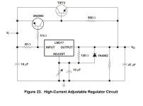
Transistors are BD140 and KD503 or MJ15003
- What about the power supply decoupling caps ? should I let them there or just use one cap per op amp from - to + ( pin 4 - 8 ) ?.
-Since you're here , please also take a quick look at this pcb I just draw,
Copper would be on the bottom , I'll just mirror it. easier to draw like this and then mirror it, also I will make them myself not send them to JLCPCB or other manufacturers. Maybe in the future, but at least for now I will make them. ( Long wait time for where I live ).
Transistors are BD140 and KD503 or MJ15003
Attachments
Shorter, more direct traces perform better (EMC-wise) as opposed to longer ones. If you don't mind the size, you could leave the extra space for the ground fill.Any benefit for being smaller ? ( besides less material wasted ) .
If you don't have the spirit to revise, just leave it at that, it should still work.
One decoupling capacitor per supply per chip. Power supply board should be OK. And it is also better to get rid of the 90* bends by replacing them with two 45* corners.- What about the power supply decoupling caps ? should I let them there or just use one cap per op amp from - to + ( pin 4 - 8 ) ?.
Should be ok for power supply.please also take a quick look at this pcb I just draw,
@newvirus2008 " One decoupling capacitor per supply per chip " So one for each rail for each chip ? or I misunderstood.
Can you explain a bit about " And it is also better to get rid of the 90* bends by replacing them with two 45* corners. " why it matters?.
Also, thank you very much for replying !.
Can you explain a bit about " And it is also better to get rid of the 90* bends by replacing them with two 45* corners. " why it matters?.
Also, thank you very much for replying !.
- Home
- Source & Line
- Analog Line Level
- Quick question about active crossover