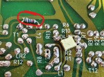
The resistor is a Dada mod, but I can't find the details. It's on both channels, but there are no problems on the right channel. You can see it here - http://quadrevisionspot.blogspot.com/2008/02/quad-306-upgrade-service-diy-kit-launch.html
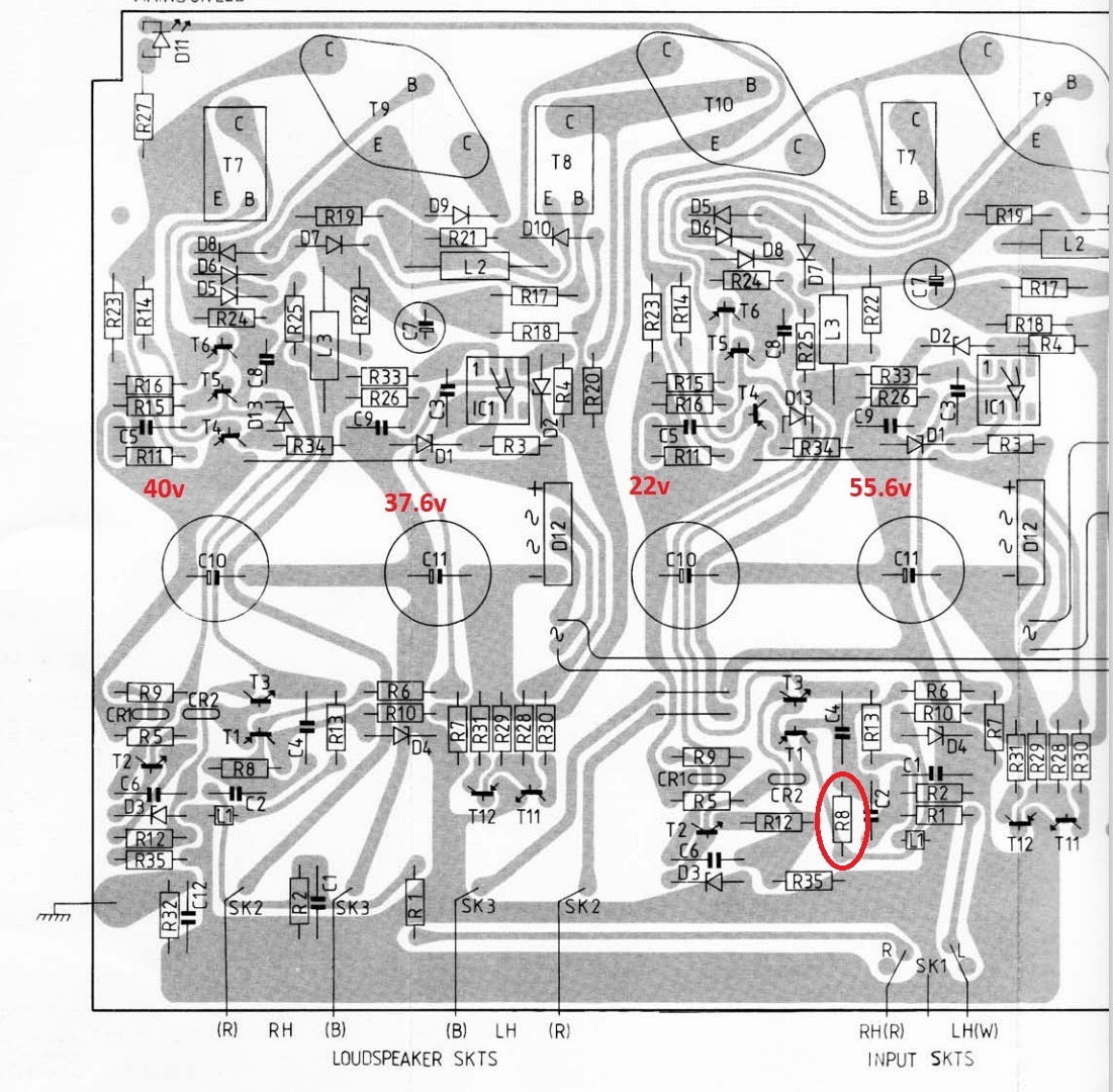
When trying to work out where to measure the voltages, I couldn't find R8 on your simulation:

When trying to work out where to measure the voltages, I couldn't find R8 on your simulation:
A couple of years ago, I tried fitting some very large coupling capacitors on flying leads. They only just fitted in the case and were fine for quite a while.
When searching my backup hard drive for any info on the Dada mods, I found something I'd written down.
Quote - "Started popping / random noises in LEFT channel. Poking L1 Inductor made pops worse (so did touching other things sometimes) but always when touching L1, Tried to measure L1 continuity in circuit, measured fine at first but not when I tried again (No reading -
strange).
Removed L1 from left channel and measured out of circuit (20uh 0.65dcr) so put back. Popping / random noises now gone, but now
hum or buzz in left channel. Gets worse when holding coupling cap or moving it outside near RCA input.
Swapped L1 from left to right channel and all seems ok (very strange)
Buzz still there with lid on or off, and with input signal cables removed.
Put the original 100nf coupling capacitors back and there is silence, even with my ear right up to the speakers."
Last edited:
Recently (last few weeks), I've noticed some odd, strange popping or rustling noises at night (hard to describe). It might only happen for a few seconds, and then I might not hear it for a few days.
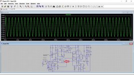
R8 on the sim was me adding the resistor I could see in your pictures. As soon as that was added the circuit gives the same fault condition as you are now describing.When trying to work out where to measure the voltages, I couldn't find R8 on your simulation:
It sounds like a lot is going on with this amp modification wise and that really makes it all a bit of an unknown. It would be worth you going back over everything you have done as well and perhaps even reverse everything back to original as a starting point. Check every single thing you have altered and changed.
I'm also going to suggest you lift one end of that resistor and see what happens to the voltages.
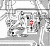
Sorry, I didn't explain very well. In post #23 there's a picture of the back of the circuit board with R8 circled in red. The R8 you added to your simulation was the Dada mod.R8 on the sim was me adding the resistor I could see in your pictures. As soon as that was added the circuit gives the same fault condition as you are now describing.
I've removed all capacitors and the two resistors from the back of the board.
T1
B 0v
C -.409v
E -.297v (was rising very slowly)
T2
B -.304v
C -29.7mV
E -29.7mV
T3
B -.286v
C -31mV
E -0v
T4
B -.296v
C -00.3mV
E -.299v
T5
B -.292v
C -0.12mV
E -.294v
T6
B -.283v
C -00.9mV
E -.283v
T7
B -.273v
C -00.7mV
E -.274
T8
B -.305v
C -.306v
E -00.7mV
T9
B -.170v
C -.279v
E -00.8mV
T10
B -.313v
C -00.8mV
E -.313v
T11
B -.285v
C -.271v
E 0v
T12
B -.285v
C -.300v
E 0v
Erm... not sure what has happened there 🙂 there is essentially no voltage anywhere with those readings. You should be seeing the full supply voltage on T8 and T9 collectors and whatever you measure there should add to the full 70 to 80 volt supply voltage.
Well, that was embarrassing. Here's the correct readings (hopefully).
T1
B -6.72v
C -6.90v
E -6.15v
T2
B 6.87v
C 20.3v
E 15.2v
T3
B -6.16v
C 20.3v
E 0.361v
T4
B 22.5v
C -00.3mV
E 22.5v
T5
B 20.3v
C 21.1v
E 21.1v
T6
B 21.1v
C 21.1v
E 21.7v
T7
B 21.6v
C 21.1v
E 22.4v
T8
B 18.9v
C -55.6v
E 19.5v
T9
B 19.4v
C 22.3v
E 19.3v
T10
B -55.1v
C 19.3v
E -55.1v
T11
B -0.588v
C 22.5v
E 0v
T12
B -0.585v
C -16mV
E 0v
Interesting, thanks 🙂
Now without having this in front of me its not easy but...
T2. +6.8 volts on the base is correct. That is fixed by the Zener. +20.3 on the collector although incorrect (it should be much higher) is still a valid reading.
The emitter volts is the puzzle here. You have it at +15 volts which means the transistor is reverse biased. What is odd is where that voltage is coming from.
So first question is whether T2 is leakey from collector to emitter. That needs checking carefully.
Don't discount anything as a cause.
There doesn't appear to be any other easy route for that voltage. C6 would have to be leaky. Could you have touched it with a hot iron and melted it? There is no other route I can see because T3 has negative voltages on the base and almost zero on the emitter.
So at face value T2 is suspect as a first option. Look all that area over very carefully if you have done work there.
🙂🙂🙂🙂🙂🙂
You're a genius!!!
Where do I send the Paypal money?
I haven't plugged it back in yet, but DC offset is now a nice low 00.1mV. The legs of C6 (polystyrene cap) were touching together. I couldn't see this because it was underneath the body of the cap. I'm so glad the caps not broken because it's copper foil and I can't find them anywhere.
🙂🙂🙂🙂🙂🙂
Do you know why the 10k resistor across the Collector and Emittor of T3 shows a fault in your simulation, but not in reality?
Do you have any opinions of replacing the 1N4003 diodes for UF4007?
Post #4 (I'm also curious about the current dumping resistor mod)
https://theartofsound.net/forum/showthread.php?40378-My-Day-improving-Audio-Equipment
Post #4 (I'm also curious about the current dumping resistor mod)
https://theartofsound.net/forum/showthread.php?40378-My-Day-improving-Audio-Equipment
- Home
- Amplifiers
- Solid State
- Quad 306 High DC offset in left channel


